Transistors, the building blocks of modern electronics, are typically made of silicon. Because it’s a semiconductor, this material can control the flow of electricity in a circuit. But silicon has fundamental physical limits that restrict how compact and energy-efficient a transistor can be.
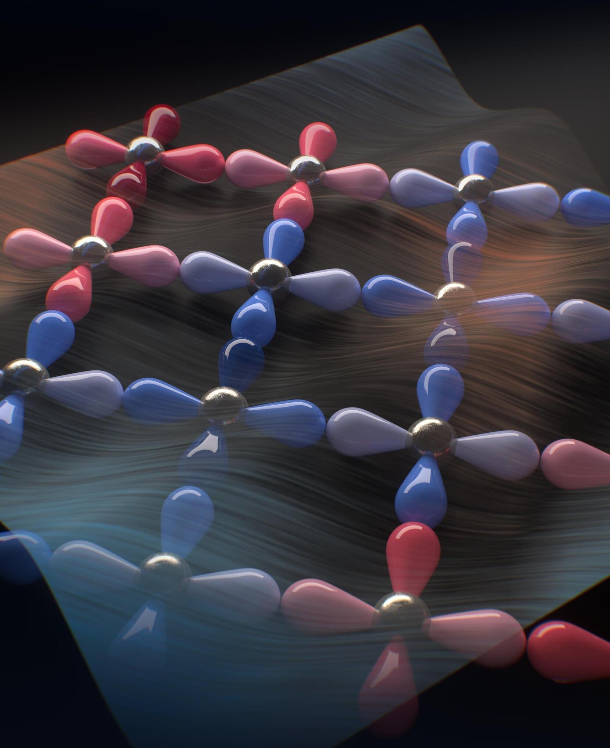
MIT researchers have now replaced silicon with a magnetic semiconductor, creating a magnetic transistor that could enable smaller, faster, and more energy-efficient circuits. The material’s magnetism strongly influences its electronic behavior, leading to more efficient control of the flow of electricity.
The team used a novel magnetic material and an optimization process that reduces the material’s defects, which boosts the transistor’s performance.


