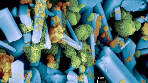
Quasicrystals (QCs) are fascinating solid materials that exhibit an intriguing atomic arrangement. Unlike regular crystals, in which atomic arrangements have an ordered repeating pattern, QCs display long-range atomic order that is not periodic. Due to this ‘quasiperiodic’ nature, QCs have unconventional symmetries that are absent in conventional crystals. Since their Nobel Prize-winning discovery, condensed matter physics researchers have dedicated immense attention towards QCs, attempting to both realize their unique quasiperiodic magnetic order and their possible applications in spintronics and magnetic refrigeration.
Although theoreticians have long expected the establishment of antiferromagnetism in select QCs, it has yet to be directly observed. Experimentally, most magnetic iQCs exhibit spin-glass-like freezing behavior, with no sign of long-range magnetic order, leading researchers to question whether antiferromagnetism is even compatible with quasiperiodicity — until now.
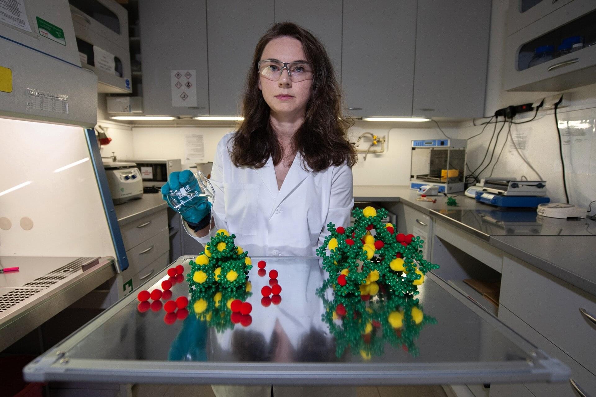
In a groundbreaking study, a research team has finally discovered antiferromagnetism in a real QC. The team was led by Ryuji Tamura from the Department of Materials Science and Technology at Tokyo University of Science (TUS), along with Takaki Abe, also from TUS, Taku J. Sato from Tohoku University, and Max Avdeev from the Australian Nuclear Science and Technology Organisation and The University of Sydney. Their study was published in the journal Nature Physics on April 11, 2025.
Quasicrystals are intriguing materials with long-range atomic order that lack periodicity. It has been a longstanding question whether antiferromagnetism, while commonly found in regular crystals, is even possible in quasicrystals. In a new study, researchers have finally answered this question, providing the first definitive neutron diffraction evidence of antiferromagnetism in a real icosahedral quasicrystal. This discovery opens a new research area of quasiperiodic antiferromagnets, with potential applications in spintronics.