NASA Glenn engineers Chirs Kantzos and Tim Smith can now call themselves inventors, too. They are the minds behind NASA’s breakthrough material, a superalloy…
Category: materials – Page 150
Neuronal representation of visual working memory content in the primate primary visual cortex
To capture a broader understanding of memory encoding, we expanded our experiments to include two other stimulus types: colors and face pictures (see Materials and Methods). Both monkeys demonstrated high accuracy in memorizing grating orientations in the “orientation DMTS” task, colors in the “color DMTS” task, and face pictures in the “face DMTS” task [DP: ~94% and DQ: ~87% versus 50%, all P < 0.01 (one-sample t test)] (fig. S1), indicating that they had been well trained.
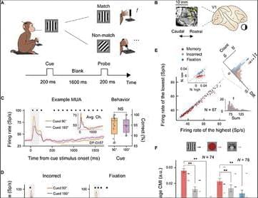
We implanted a Utah array in each monkey’s V1 area (see Materials and Methods; Fig. 1B) and presented the stimuli onto the receptive field (RF) centers of the recorded neurons (fig. S2, A and D). This enabled simultaneous monitoring of neuronal activity in our experiments. Our analyses focused primarily on neuronal activity before probe stimulus onset.
Representative neuronal responses for two of the VWM content conditions in the orientation DMTS task at a selected electrode are shown in Fig. 1C. During the stimulus period (0 to 200 ms after cue onset), neurons displayed distinct firing patterns between the two content conditions (90° or 180° orientation). An off-response emerged following the cue offset, and activity gradually diminished. During the delay period, defined as 700 to 1,700 ms after cue onset (the thick gray line in Fig. 1C), neurons also exhibited a significant difference in firing rate between the two content conditions (N = 1,810 trials for 90°; N = 1,865 trials for 180°; all marked positions P < 0.01) without any behavioral performance bias (N = 16 sessions, P = 0.94; right panel in Fig. 1C). The difference in response between these two content conditions during the delay period at the same electrode was less prominent in incorrect-response trials and in the fixation task (Fig. 1D).
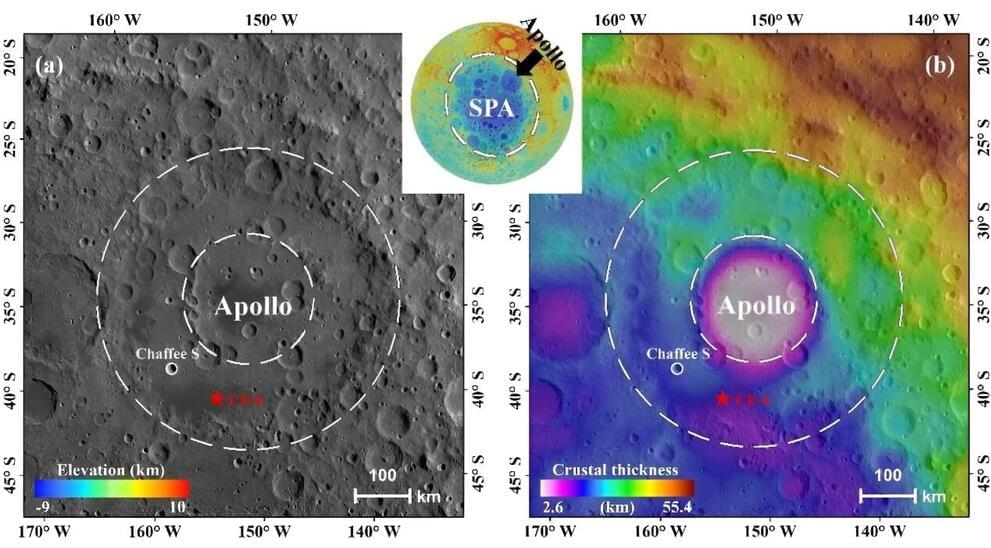
Geologists expect Chang’e-6 lunar surface samples to contain volcanic rock and impact ejecta
On June 25, China’s Chang’e-6 (CE-6) lunar probe is set to return to Earth, carrying the first surface samples collected from the farside of the moon. In anticipation of this historic event, scientists from the Institute of Geology and Geophysics at the Chinese Academy of Sciences are publishing their predictions for the unique materials that may be found in the CE-6 samples in the journal The Innovation.
Space radiation can damage satellites—next-generation material could self-heal when exposed to cosmic rays
The space environment is harsh and full of extreme radiation. Scientists designing spacecraft and satellites need materials that can withstand these conditions.
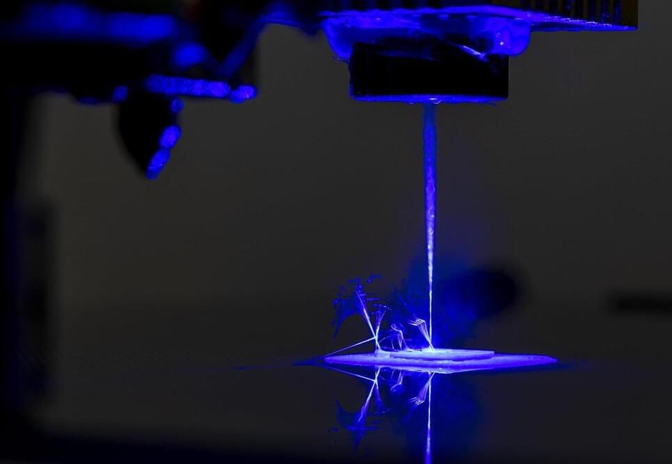
No assembly required: Innovative 3D printing method streamlines multi-materials manufacturing
University of Missouri researchers have developed a way to create complex devices with multiple materials—including plastics, metals and semiconductors—all with a single machine.
The research, which was recently published in Nature Communications, outlines a novel 3D printing and laser process to manufacture multi-material, multi-layered sensors, circuit boards and even textiles with electronic components.
It’s called the Freeform Multi-material Assembly Process, and it promises to revolutionize the fabrication of new products.
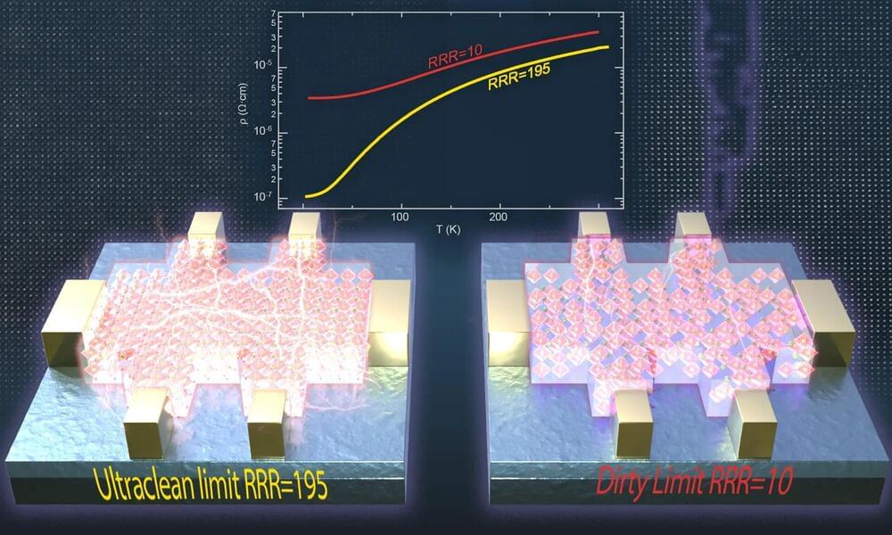
New research uncovers hidden phenomena in ultra-clean quantum materials
In a paper published today in Nature Communications, researchers unveiled previously unobserved phenomena in an ultra-clean sample of the correlated metal SrVO3. The study offers experimental insights that challenge the prevailing theoretical models of these unusual metals.
The international research team—from the Paul Drude Institute of Solid State Electronics (PDI), Germany; Oak Ridge National Laboratory (ORNL); Pennsylvania State University; University of Pittsburgh; the Pittsburgh Quantum Institute; and University of Minnesota—believes their findings will prompt a re-evaluation of current theories on electron correlation effects, shedding light on the origins of valuable phenomena in these systems, including magnetic properties, high-temperature superconductivity, and the unique characteristics of highly unusual transparent metals.
The perovskite oxide material SrVO3 is classified as a Fermi liquid—a state describing a system of interacting electrons in a metal at sufficiently low temperatures.
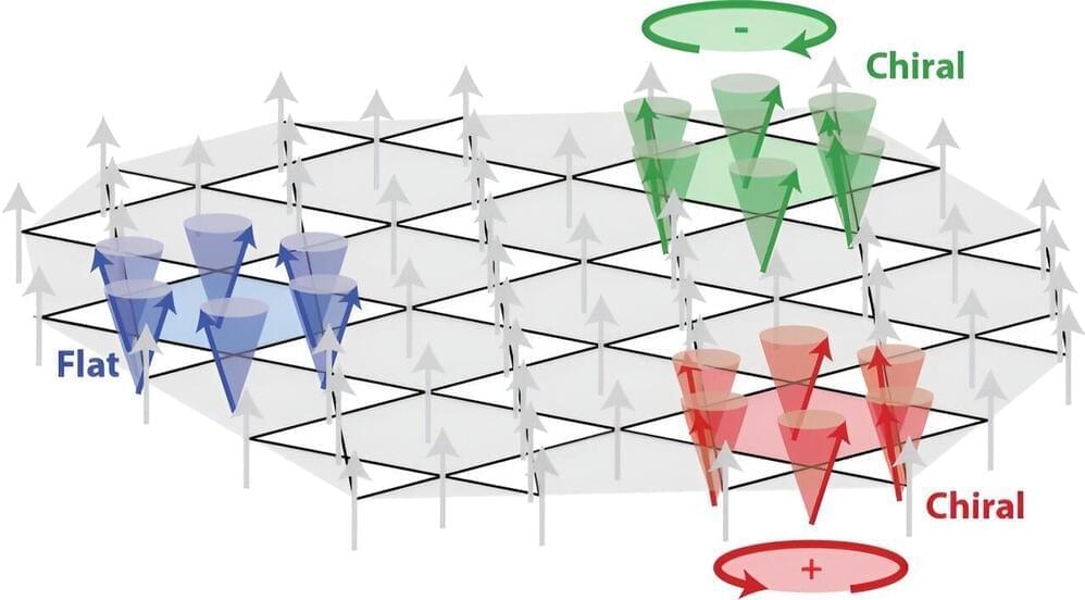
Researchers find unexpected excitations in a kagome layered material
“People are always searching for chiral ground states,” McQueeney said. “The reason we use the concept of quasiparticle here is because it is a way of transmitting energy or information, like an electron is a quasiparticle, and we can send it from point A to point B, carrying some information.
A chiral quasiparticle would have other attributes to it. It would have a handedness, for example, and so you could think about novel ways to, say, transmit information from point A to point B, which didn’t involve moving a charge, but moving some chiral signal.
Discovering this new chiral excitation was especially exciting for McQueeney, You don’t expect it to be there, he said. And we still don’t understand why it’s there. As a matter of fact, we’re setting up other experiments to look for it in other materials.

Terahertz Waves Supercharged: A Breakthrough With Magnetic Materials
Positioned between microwaves and infrared light, terahertz waves are key to pioneering advancements in imaging and diagnostic technologies. A recent discovery at Tohoku University of a material that can emit these waves more intensely promises to catalyze significant breakthroughs across a spectrum of industries.
Terahertz waves are being intensely studied by researchers around the world seeking to understand the “terahertz gap.” Terahertz waves have a specific frequency that put them somewhere between microwaves and infrared light. This range is referred to as a “gap” because much remains unknown about these waves. In fact, it was only relatively recently that researchers were able to develop the technology to generate them. Researchers at Tohoku University have brought us closer to understanding these waves and filling in this gap of knowledge.
Breakthrough in Terahertz Wave Generation.

Controlling Electronics With Light: Magnetite’s Hidden Phases Exposed by Lasers
Researchers have successfully manipulated the structural properties of magnetite using light-induced phase transitions.
This technique uncovered hidden phases of magnetite, paving the way for new approaches to material manipulation in electronics.
Breakthrough in magnetite phase transition research.
Apple partner’s new material boosts solid-state batteries by 100x
Japanese firm TDK aims to improve next-gen solid-state battery design with a new material utilizing multi-layer lamination technology.