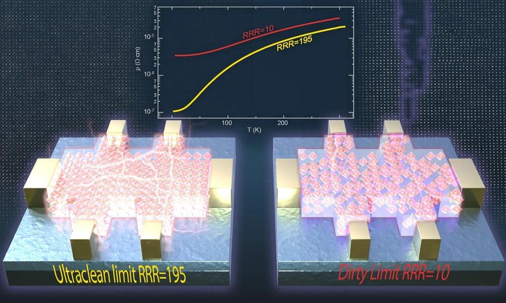
Menu

Blog

Archive for the ‘materials’ category: Page 147

Jun 15, 2021

New graphene display creates LEDs at an atomic level

Posted by in category: materials

Circa 2015 o,.o!


New graphene displays could pave the way for ultra-thin, incredibly durable, and highly efficient LCD technology — even at this early state of development.

Jun 15, 2021

Light-squashing spaceplates could lead to paper-thin smartphones

Posted by in categories: materials, mobile phones

Material layers compress empty space between optical components.

Jun 14, 2021

Israeli scientists show they can shrink optical technology by 1,000 times

Posted by in category: materials

Trapping and observing light in super-thin materials, Technion researchers say their work may pave way for new generation of tiny light-powered tech.

Jun 13, 2021

Graphene Hard Drives Store Ten Times as Much Data

Posted by in categories: computing, materials

Another day, another problem solved by coating something in graphene.

Jun 8, 2021

Ultra-high-density hard drives made with graphene store ten times more data

Posted by in categories: computing, materials

Graphene can be used for ultra-high density hard disk drives (HDD), with up to a tenfold jump compared to current technologies, researchers at the Cambridge Graphene Center have shown.

The study, published in Nature Communications, was carried out in collaboration with teams at the University of Exeter, India, Switzerland, Singapore, and the US.

HDDs first appeared in the 1950s, but their use as in personal computers only took off from the mid-1980s. They have become ever smaller in size, and denser in terms of the number of stored bytes. While solid state drives are popular for mobile devices, HDDs continue to be used to store files in desktop computers, largely due to their favorable cost to produce and purchase.

Jun 7, 2021

Highly Effective New Way Developed to Paint Complex 3D-Printed Objects

Posted by in categories: biotech/medical, materials

Rutgers engineers have created a highly effective way to paint complex 3D-printed objects, such as lightweight frames for aircraft and biomedical stents, that could save manufacturers time and money and provide new opportunities to create “smart skins” for printed parts.

The findings are published in the journal ACS Applied Materials & Interfaces.

Conventional sprays and brushes can’t reach all nooks and crannies in complex 3D-printed objects, but the new technique coats any exposed surface and fosters rapid prototyping.

Jun 4, 2021

Magnetism drives metals to insulators in new experiment

Posted by in categories: materials, physics

Like all metals, silver, copper, and gold are conductors. Electrons flow across them, carrying heat and electricity. While gold is a good conductor under any conditions, some materials have the property of behaving like metal conductors only if temperatures are high enough; at low temperatures, they act like insulators and do not do a good job of carrying electricity. In other words, these unusual materials go from acting like a chunk of gold to acting like a piece of wood as temperatures are lowered. Physicists have developed theories to explain this so-called metal-insulator transition, but the mechanisms behind the transitions are not always clear.

“In some cases, it is not easy to predict whether a material is a or an insulator,” explains Caltech visiting associate Yejun Feng of the Okinawa Institute for Science and Technology Graduate University. “Metals are always good conductors no matter what, but some other so-called apparent metals are insulators for reasons that are not well understood.” Feng has puzzled over this question for at least five years; others on his team, such as collaborator David Mandrus at the University of Tennessee, have thought about the problem for more than two decades.

Now, a new study from Feng and colleagues, published in Nature Communications, offers the cleanest experimental proof yet of a theory proposed 70 years ago by physicist John Slater. According to that theory, magnetism, which results when the so-called “spins” of electrons in a material are organized in an orderly fashion, can solely drive the metal-insulator transition; in other previous experiments, changes in the lattice structure of a material or based on their charges have been deemed responsible.

Jun 4, 2021

Ultra-thin lithium offers a solid platform for high-capacity batteries

Posted by in categories: energy, materials

Scientists in South Korea have made a breakthrough in battery research that could help us bust through a key bottleneck in energy storage. The team’s advance overcomes a technical issue that has held back highly promising lithium-metal battery architecture and could pave the way for batteries with as much as 10 times the capacity of today’s devices.

The reason lithium-metal batteries hold so much promise is because of the excellent energy density of pure lithium metal. Scientists hope to swap out the graphite used for the anode in today’s lithium batteries for this “dream material,” though this comes with some complicated problems to solve.

One of the key issues relates to needle-like structures called dendrites, which form on the anode surface as the battery is charged. These penetrate the barrier between the anode and the battery’s other electrode, the cathode, and quickly cause the battery to short-circuit, fail, or even catch fire.

Jun 2, 2021

Motion of water monomers reveals a kinetic barrier to ice nucleation on graphene

Posted by in category: materials

The dynamics of water molecules at interfaces controls natural and artificial processes, but experimental investigations have been challenging. Here the authors investigate water molecules on a graphene surface using helium spin-echo spectroscopy, and reveal a regime where freely mobile molecules undergo strong repulsive mutual interactions which inhibit ice nucleation.

Jun 1, 2021

Future of chip making to lean heavily on AI for spotting defects, says Applied Materials

Posted by in categories: materials, robotics/AI

Enlight uses light polarization to maximize resolution and to find critical defects in half the time of the typical optical scanner. The scanner for the first time will capture both direct light bouncing off the wafer surface, and scattered light, known as “brightfield” and “greyfield,” respectively. That’s like scanning two things in one pass, cutting in half the time required.