A research team led by Professor Jang-Sik Lee from the Department of Materials Science and Engineering and the Department of Semiconductor Engineering at Pohang University of Science and Technology (POSTECH) has significantly enhanced the data storage capacity of ferroelectric memory devices. By utilizing hafnia-based ferroelectric materials and an innovative device structure, their findings, published on June 7 in the international journal Science Advances, mark a substantial advancement in memory technology.
With the exponential growth in data production and processing due to advancements in electronics and artificial intelligence (AI), the importance of data storage technologies has surged. NAND flash memory, one of the most prevalent technologies for mass data storage, can store more data in the same area by stacking cells in a three-dimensional structure rather than a planar one. However, this approach relies on charge traps to store data, which results in higher operating voltages and slower speeds.
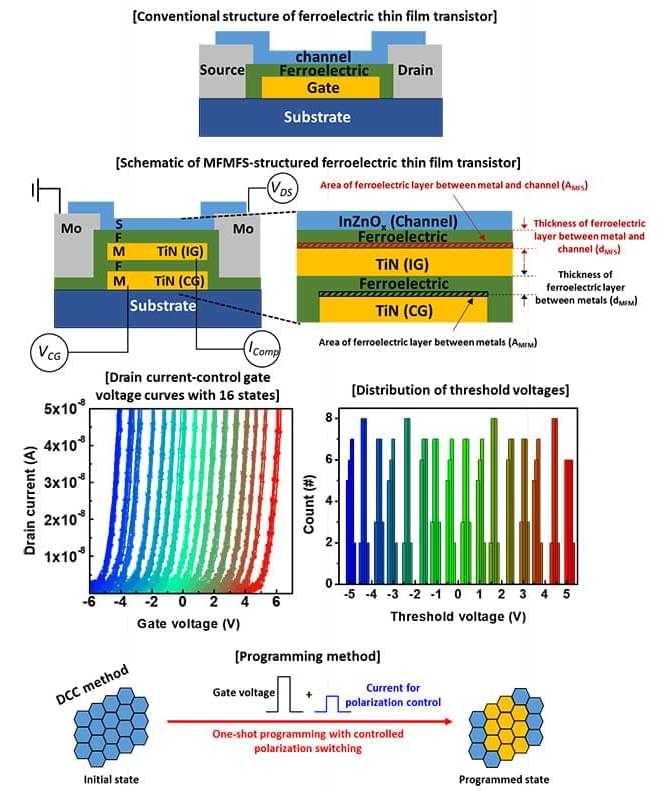
Recently, hafnia-based ferroelectric memory has emerged as a promising next-generation memory technology. Hafnia (Hafnium oxide) enables ferroelectric memories to operate at low voltages and high speeds. However, a significant challenge has been the limited memory window for multilevel data storage.