This cabin in the woods is an otherworldly, all-black, geometric structure built to provide cozy refuge even in harsh Finnish winters. It was designed for a California-based CEO who returned home to Finland with her family to be closer to her ancestral land so she could maintain it. The cabin is aptly named Meteorite based on its unique shape and is set in a clearing surrounded by spruce and birch trees. The cabin is made entirely from cross-laminated timber (CLT) which is a sustainable alternative to other construction materials.
Category: materials – Page 153
Typically, the key goal of electronics engineers is to develop components and devices that are durable and can operate for long periods of time without being damaged. Such devices require resistant materials, which ultimately contribute to the accumulation of electronic waste on our planet.
Researchers at Northwestern University and the University of Illinois have been conducting research focusing on an entirely different type of electromechanical system (MEMS): those based on so-called “transient materials.” Transient materials are materials that can dissolve, resorb, disintegrate or physically disappear in other ways at programmed and specific times.
Their most recent paper, published in Nature Electronics, introduces new MEMS based on fully water-soluble materials that could dissolve in their surrounding environment after set periods of time. In the future, these materials could help to decrease the amount of electronic waste, enabling the development of some electronic devices that spontaneously disappear when they are no longer needed.
A team of researchers at the Chinese Academy of Sciences, has developed an artificial finger that was able to identify certain surface materials with 90% accuracy. In their paper published in the journal Science Advances, the group describes how they used triboelectric sensors to give their test finger an ability to gain a sense of touch.
Prior research has led to the development of robotic fingers that have the ability to recognize certain attributes of certain surfaces, such as pressure or temperature—the team with this new effort, have taken such efforts further by adding the ability to identify a material that is being touched.
The finger was created by applying small square sensors to the tip of a finger-shaped object. Each of the squares was made of a different kind of plastic polymer, each chosen because of their unique electrical properties. When such sensors are moved close to an object, such as a flat surface, electrons from the sensors interact with the materials in unique ways.
More people are swapping real lawns for fake but experts are worried about its environmental impact.
Circa 2019
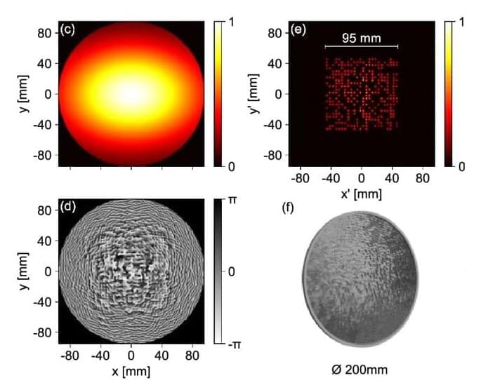
Mechanical stability of macroscopic structures on the millimetre-, centimetre-and even metre-scale could be realized by tailoring the anisotropy of light scattering along the object’s surface, without needing to focus incident light or excessively constrain the shape, size or material composition of the object.
Semiconductors in the Spotlight
Posted in electronics, materials
A new model suggests that lattice defects are responsible for the way some semiconductors become harder under illumination.
Understanding how semiconductors respond to illumination has been crucial to the development of photovoltaics and optical sensors. But some light-induced behaviors have been less thoroughly investigated. For example, when some semiconductors are illuminated, their mechanical properties can change drastically, a phenomenon known as photoelasticity. Photoelastic materials could be useful in the development of flexible electronics, but researchers do not understand in detail the mechanism behind the effect. Now, based on experiments and simulations, Rafael Jaramillo of the Massachusetts Institute of Technology and colleagues present a new theoretical framework that explains photoelasticity in terms of lattice defects [1].
The researchers used a diamond-tipped probe to make nanometer-scale indentations in samples of zinc oxide, zinc sulfide, and cadmium sulfide—first in the dark, and then under a range of visible and ultraviolet wavelengths. All three materials hardened to varying degrees when illuminated, with cadmium sulfide showing the largest and most consistent response. For every sample, the effect increased as the photon energy increased toward the material’s band gap.
Japanese studio Nendo has created an archive to house its products and furniture from precast concrete box culverts in central Japan.
Named Culvert Guesthouse, the archive and residence was constructed from four tunnel-like forms that were stacked on top of each other.
Designed by the studio as its own archive, the distinctive-shaped building is located in dense woodland on the edge of the town of Miyota in Nagano Prefecture.
A breakthrough from Deakin University researchers could help address a major obstacle in the development of environmentally-friendly, cost effective, polymer-based batteries.
The team from Deakin’s Institute for Frontier Materials (IFM) used computer modeling and simulations to design a new type of solid-state polymer electrolyte, showing its potential use in various types of polymer-based solid-state batteries, particularly sodium and potassium batteries.
Polymer-based batteries are able to support high-energy density metals in an all solid-state batteries. They use polymer as the ion conductor rather than flammable organic liquid solvents in current lithium-ion batteries. Therefore, a polymer-based solid-state battery offers an energy storage option that is greener, safer and providing a higher capacity, meaning more energy.
Potential applications include pressure-monitoring bandages, shade-shifting fabrics.
The bright iridescent colors in butterfly wings or beetle shells don’t come from any pigment molecules but from how the wings are structured—a naturally occurring example of what physicists call photonic crystals. Scientists can make their own structural colored materials in the lab, but it can be challenging to scale up the process for commercial applications without sacrificing optical precision.