This flying camera drone will put your selfie skills to shame. Buy it here: https://amzn.to/2xvPgDp
Category: electronics – Page 89


Detecting Methane from Miles Away
A new laser-based field instrument developed by a collaborative team of researchers can quantify methane leaks as tiny as 1/4 of a human exhalation from nearly…a mile away. The system, constructed around a dual-frequency comb spectrometer, provides efficient, accurate data collection at a fraction of the cost of previous technologies. The research was partially funded by DARPA’s Spectral Combs from UV to THz (SCOUT) program.
The travelling speed camera
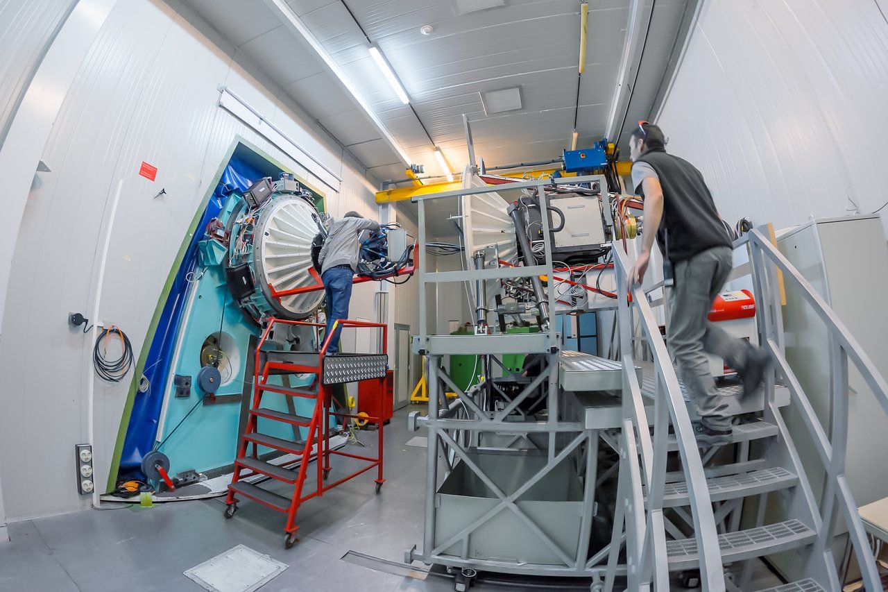
The ULTRACAM has been a staple in ESO for almost 16 years. This high-speed camera is able to do 500 photographs per second in three different wavelengths and, since 2002 has been operating at the William Herschel Telescope at La Palma (Canary Islands, Spain), the New Technology Telescope at La Silla (Chile) (where this picture was taken) and, most recently, at the Very Large Telescope at Paranal (Chile) and the Thai National Telescope at Chiang Mai (Thailand).
Some of its past targets have included: the study of black holes, “hot-Jupiters” or variable stars.

Worn Like a Helmet, a New Brain Scanner Aims to Make It Easier to Treat Kids with Epilepsy
Lightweight equipment is not much larger than what a bicyclist would wear.
- By Megan Thielking, STAT on March 22, 2018
World’s tallest active geyser may be erupting deep in Yellowstone National Park
The tallest active geyser in the world may be erupting for the first time since 2014, according to the National Park Service.
Yellowstone National Park employees reported seeing the Steamboat Geyser erupt on Thursday evening, the park service announced Friday. Park geologists then compared the accounts to thermal sensors in the area and determined it “could be a series of minor eruptions.”
The geyser can shoot water higher than 300 feet during major eruptions, according to the Park Service. A geyser in New Zealand has sent water higher, but not in more than 100 years.
MIT Engineers Have Built a Device That Pulls Electricity Out of Thin Air
Temperature changes large and small are happening around us all the time, and scientists have come up with a machine that can convert those fluctuations into electricity, potentially powering sensors and communication devices almost out of thin air.
The energy harvesting is done through what’s called a thermal resonator: a device that captures heat on one side and radiates it over to the other. As both sides try and reach equilibrium, the energy can be caught using the process of thermoelectrics.
According to the team from the Massachusetts Institute of Technology, the new thermal resonator could keep remote sensors or any off-grid devices powered up for years, just by using temperature swings – like the natural ones between night and day, for instance.

Super flexible TV display rolls up for storage
Finally, a TV display you can roll up and take with you.