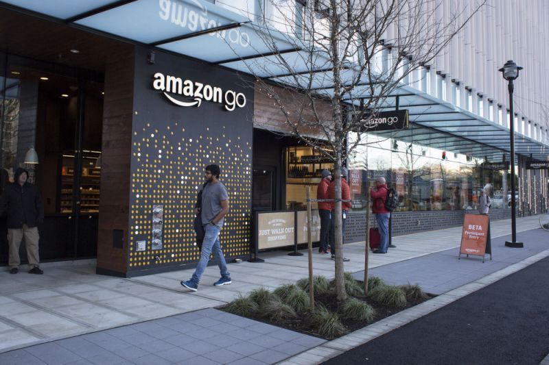
Toggle light / dark theme

X2 Biosystems awarded

They deserve it too.


X2 Biosystems has received the Society for Brain Mapping and Therapeutics (SBMT) 2016 Pioneer in Healthcare Technology Innovations Award for developing its next-generation head impact measurement sensor technology, the company said.

X2´s “X-Patch” wearable impact sensor has become widely deployed and tested head impact monitoring device, used in a continually expanding range of athletic activities from football (youth, high school, collegiate, pro) to hockey, soccer, lacrosse, rugby, Australian rules football, baseball, field hockey, wrestling, boxing, taekwondo, mixed martial arts, skiing and BMX cycling.

The X-Patch is also being actively evaluated for use in military training applications.

IIT to Develop Nanosensors to Boost Farm Productivity

Nice


HYDERABAD: In an initiative that may improve farm productivity, Indian Institute of Technology (IIT), Mumbai and Professor Jayashankar Telangana State Agriculture University (PJTSAU), Hyderabad have joined hands to develop nanosensors that can read the percentage of moisture and nutrients in the soil. This new research is expected to provide an important technological innovation in the field of agriculture. This is for the first time an IIT is collaborating with an agricultural university to devise solutions for the farmers.

“While we were exploring the possibilities of nano technology in various fields, the idea of using it in agriculture sector struck us. Thanks to the interest shown by some agricultural scientists at PJTSAU, we decided to develop nanosensors which can calculate the moisture content of the soil. There is a need for IITs to work for solving the problems faced by farmers and this is a step in that direction,” said V Ramgopal Rao, director of IIT Delhi, who was instrumental in initiating the research project, while he was the chief investigator of Centre of Excellence in Nanoelectronics Project at IIT, Mumbai.

While IIT, Mumbai will develop the nano soil sensors, PJTSAU will serve as the testing partner and conduct field tests to assess the efficacy of nanosensors. Already, funds have been allotted by IIT for the research project and a team of agricultural scientists and technologists has been formed to work on the project.

All of the technology is nearly ready for megawatt space based laser systems for science and planetary defense

California Polytechnic State University researchers propose a system capable of probing the molecular composition of cold solar system targets such as asteroids, comets, planets and moons from a distant vantage.

Their concept utilizes a directed energy beam to vaporize or sublimate a spot on a distant target, such as from a spacecraft near the object. With sufficient flux, our published results indicate that the spot temperature rises rapidly, and evaporation of materials on the target surface occurs (Hughes et al., 2015; Lubin and Hughes, 2015; Lubin et al., 2014). The melted spot serves as a high-temperature blackbody source, and ejected material creates a molecular plume in front of the spot. Molecular and atomic absorption of the blackbody radiation occurs within the ejected plume. Bulk composition of the surface material is investigated by using a spectrometer to view the heated spot through the ejected material. They envision a spacecraft that could be sent to probe the composition of a target asteroid, comet or other planetary body while orbiting the targeted object. The spacecraft would be equipped with an array of lasers and a spectrometer, powered by photovoltaics. Spatial composition maps could be created by scanning the directed energy beam across the surface. Applying the laser beam to a single spot continuously produces a borehole, and shallow sub-surface composition profiling is also possible.

Their initial simulations of laser heating, plume opacity, material absorption profiles and spectral detectivity show promise for molecular composition analysis. Such a system has compelling potential benefit for solar system exploration by establishing the capability to directly interrogate the bulk composition of objects from a distant vantage. They propose to develop models, execute preliminary feasibility analysis, and specify a spacecraft system architecture for a hypothetical mission that seeks to perform surface molecular composition analysis and mapping of a near-earth asteroid (NEA) while the craft orbits the asteroid.

New Remarkably Thin E-Skin Turns Your Body Into a Walking Display

University of Tokyo researchers have created an ultrathin and ultraflexible organic e-skin that supports PLED and OLED displays.

Researchers from the University of Tokyo have created a protective layer of organic material that’s ultrathin and ultraflexible. And the have demonstrated the material’s usefulness by making an OLED display that’s air-stable. This opens the possibility of developing better electronic skin displays, the next major leap in wearable technology.

The thickness (or rather, thinness) and flexibility of wearable electronics is an essential factor in its further development. Plastic substrates are commonly used in the creation of such devices, which still require millimeter-scale thick glass. Also, whenever micrometer-scale and flexible organic materials are developed, they aren’t reliably stable when exposed to air.

Clothes that Transmit Digital Data Are Coming

Imagine shirts that act as antennas for smartphones or tablets, workout clothes that monitor fitness level or even a flexible fabric cap that senses activity in the brain!

All this will soon be possible as the researchers working on wearable electronics have been able to embroider circuits into fabric with super precision — a key step toward the design of clothes that gather, store or transmit digital information.

“A revolution is happening in the textile industry. We believe that functional textiles are an enabling technology for communications and sensing and one day, even for medical applications like imaging and health monitoring,” said lead researcher John Volakis from Ohio State University.

New hybrid inks permit printed, flexible electronics without sintering

Research scientists at INM have combined the benefits of organic and inorganic electronic materials in a new type of hybrid inks. This allows electronic circuits to be applied to paper directly from a pen, for example.

The electronics of the future will be printed. Flexible circuits can be produced inexpensively on foil or paper using printing processes and permit futuristic designs with curved diodes or input elements. This requires printable electronic materials that can be printed and retain a high level of conductivity during usage in spite of their curved surfaces. Some tried and tested materials include organic, conductive polymers and nanoparticles made of conductive oxides (TCOs). Research scientists at INM – Leibniz-Institute for New Materials have now combined the benefits of organic and inorganic electronic materials in a new type of hybrid inks. This allows electronic circuits to be applied to paper directly from a pen, for example.

hybrid inks permit printed, flexible electronics without sintering

New hybrid inks permit printed, flexible electronics without sintering. (Image: INM)

HRL to develop inertial sensor tech for DARPA

Could this sensor technology revolutionize how auto and other navigation technology looks in the future?


The Defense Advanced Research Projects Agency (DARPA) has awarded HRL Laboratories $4.3 million to develop vibration- and shock-tolerant inertial sensor technology that enables future system accuracy needs without utilizing GPS.

While GPS provides sub-meter accuracy in optimal conditions, the signal is often lost or degraded due to natural interference or malicious jamming.

HRL Laboratories, based in Malibu, California, is a corporate research-and-development laboratory owned by The Boeing Company and General Motors specializing in research into sensors and materials, information and systems sciences, applied electromagnetics and microelectronics.

Berkeley Lab captures first high-res 3D images of DNA segments | KurzweilAI

“DNA base pairing has been used for many years to direct the arrangement of inorganic nanocrystals into small groupings and arrays with tailored optical and electrical properties. The control of DNA-mediated assembly depends crucially on a better understanding of three-dimensional structure of DNA-nanocrystal-hybridized building blocks. Existing techniques do not allow for structural determination of these flexible and heterogeneous samples.”

Read more