Researchers at the University of Washington have developed 3D-printed objects that can transmit and store data about their use without the need for batteries or electronics.
Category: electronics – Page 86
World’s first full-body medical scanner generates astonishing 3D images
After over a decade of development, the world’s first full-body medical scanner has produced its first images. The groundbreaking imaging device is almost 40 times faster than current PET scans and can capture a 3D picture of the entire human body in one instant scan.

Drone’s high-tech bike theft attempt caught on camera
Nov. 12 (UPI) — A group of shocked cyclists captured video of the moment a drone operator nearly pulled off a high-tech bike theft.
The video, recorded in Hustopece, Moravia, Czech Republic, shows the cyclists climbing a local landmark known as Lookout Tower and taking video of a drone flying nearby.
The cyclists start scrambling down the tower when the drone lowers down to the ground and picks up one of the bicycles.

Samsung will soon test TVs that can be controlled with your brain
Samsung TVs are already some of the most popular options for high-end home theater systems, and the company is now using its television-making prowess to help people with disabilities live more normal lives. A new project by a Samsung team in Switzerland could yield the first smart TV that can be controlled with thoughts.
As CNET reports, Samsung has partnered with Swiss scientists to bring the system to life. Called ‘Project Pontis,’ the ultimate goal is to build a brain/software interface that will allow individuals with movement disabilities to control television features like channel switching and volume control with their brains rather than their bodies.

Nanocrystals arrange to improve electronics
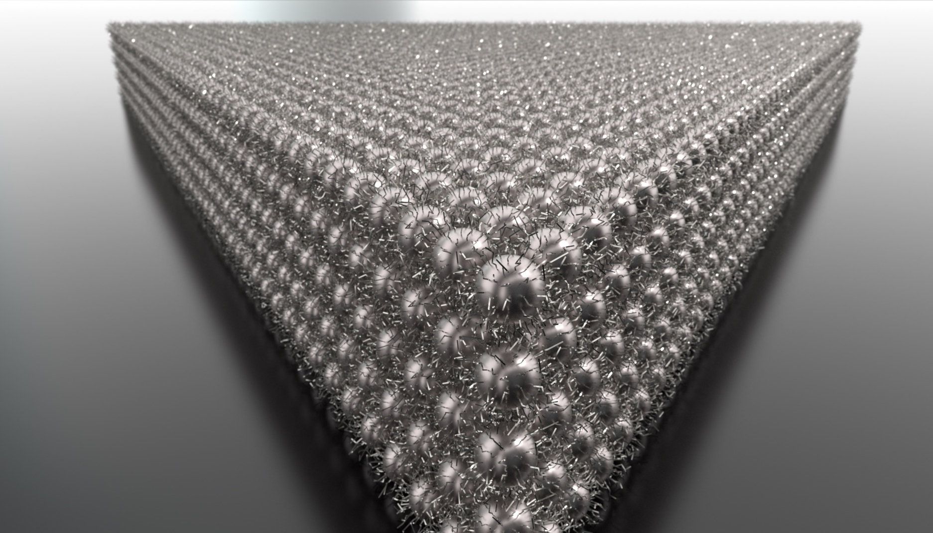
Lawrence Livermore National Laboratory (LLNL) researchers are working to make better electronic devices by delving into the way nanocrystals are arranged inside of them.
Nanocrystals are promising building blocks for new and improved electronic devices, due to their size-tunable properties and ability to integrate into devices at low-cost.
While the structure of nanocrystals has been extensively studied, no one has been able to watch the full assembly process.

How to Watch Apple’s ‘Gather Round’ iPhone Event Live in Your Time Zone
There’s just a day to go until Apple holds its annual iPhone-centric event to introduce new iPhone models, with this year’s event expected to see the debut of the 5.8-inch OLED iPhone Xs, the 6.5-inch OLED iPhone Xs Max, and the 6.1-inch LCD iPhone, which could be called the iPhone Xr.
We’re also expecting to see new Apple Watch Series 4 models with larger displays thanks to reduced bezels and more accurate ECG-based heart monitoring technology. Other surprises could be in the works too, such as the launch of new second-generation AirPods and the debut of the long-awaited AirPower.
Novel optics for ultrafast cameras create new possibilities for imaging
MIT researchers have developed novel photography optics that capture images based on the timing of reflecting light inside the optics, instead of the traditional approach that relies on the arrangement of optical components. These new principles, the researchers say, open doors to new capabilities for time- or depth-sensitive cameras, which are not possible with conventional photography optics.
Specifically, the researchers designed new optics for an ultrafast sensor called a streak camera that resolves images from ultrashort pulses of light. Streak cameras and other ultrafast cameras have been used to make a trillion-frame-per-second video, scan through closed books, and provide depth map of a 3D scene, among other applications. Such cameras have relied on conventional optics, which have various design constraints. For example, a lens with a given focal length, measured in millimeters or centimeters, has to sit at a distance from an imaging sensor equal to or greater than that focal length to capture an image. This basically means the lenses must be very long.
In a paper published in this week’s Nature Photonics, MIT Media Lab researchers describe a technique that makes a light signal reflect back and forth off carefully positioned mirrors inside the lens system. A fast imaging sensor captures a separate image at each reflection time. The result is a sequence of images—each corresponding to a different point in time, and to a different distance from the lens. Each image can be accessed at its specific time. The researchers have coined this technique “time-folded optics.”


CT scanners on trial at Heathrow could bring end to liquids ban
New technology could mean passengers would no longer need to remove items from hand luggage for screening.

Engineers develop origami electronics from cheap, foldable paper
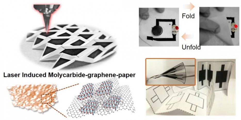
UC Berkeley engineers have given new meaning to the term “working paper.” Using inexpensive materials, they have fabricated foldable electronic switches and sensors directly onto paper, along with prototype generators, supercapacitors and other electronic devices for a range of applications.
Research to develop paper electronics has accelerated in the last 10 years. Besides its availability and low cost, paper offers an intriguing potential: simply folding it could switch circuits on and off or otherwise change their activity—a kind of electronic origami.
But most efforts to fabricate electrodes onto paper with sufficient conductivity for practical use have employed expensive metals such as gold or silver as the conducting material, swamping the potential savings of paper as a substrate.
