Toggle light / dark theme

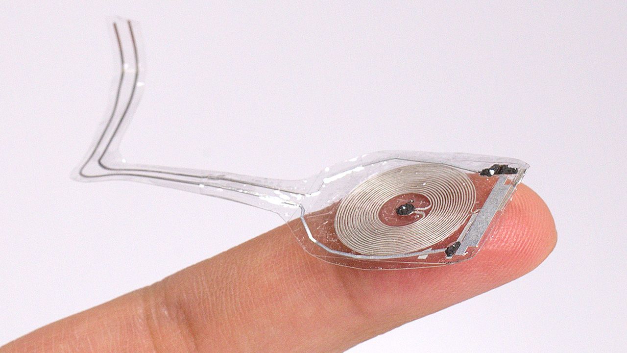
University of Tokyo researchers have created an ultrathin and ultraflexible organic e-skin that supports PLED and OLED displays.

Researchers from the University of Tokyo have created a protective layer of organic material that’s ultrathin and ultraflexible. And the have demonstrated the material’s usefulness by making an OLED display that’s air-stable. This opens the possibility of developing better electronic skin displays, the next major leap in wearable technology.

The thickness (or rather, thinness) and flexibility of wearable electronics is an essential factor in its further development. Plastic substrates are commonly used in the creation of such devices, which still require millimeter-scale thick glass. Also, whenever micrometer-scale and flexible organic materials are developed, they aren’t reliably stable when exposed to air.

Read more

Imagine shirts that act as antennas for smartphones or tablets, workout clothes that monitor fitness level or even a flexible fabric cap that senses activity in the brain!

All this will soon be possible as the researchers working on wearable electronics have been able to embroider circuits into fabric with super precision — a key step toward the design of clothes that gather, store or transmit digital information.

“A revolution is happening in the textile industry. We believe that functional textiles are an enabling technology for communications and sensing and one day, even for medical applications like imaging and health monitoring,” said lead researcher John Volakis from Ohio State University.

Read more

Research scientists at INM have combined the benefits of organic and inorganic electronic materials in a new type of hybrid inks. This allows electronic circuits to be applied to paper directly from a pen, for example.

The electronics of the future will be printed. Flexible circuits can be produced inexpensively on foil or paper using printing processes and permit futuristic designs with curved diodes or input elements. This requires printable electronic materials that can be printed and retain a high level of conductivity during usage in spite of their curved surfaces. Some tried and tested materials include organic, conductive polymers and nanoparticles made of conductive oxides (TCOs). Research scientists at INM – Leibniz-Institute for New Materials have now combined the benefits of organic and inorganic electronic materials in a new type of hybrid inks. This allows electronic circuits to be applied to paper directly from a pen, for example.

hybrid inks permit printed, flexible electronics without sintering

New hybrid inks permit printed, flexible electronics without sintering. (Image: INM)

Read more

Could this sensor technology revolutionize how auto and other navigation technology looks in the future?


The Defense Advanced Research Projects Agency (DARPA) has awarded HRL Laboratories $4.3 million to develop vibration- and shock-tolerant inertial sensor technology that enables future system accuracy needs without utilizing GPS.

While GPS provides sub-meter accuracy in optimal conditions, the signal is often lost or degraded due to natural interference or malicious jamming.

HRL Laboratories, based in Malibu, California, is a corporate research-and-development laboratory owned by The Boeing Company and General Motors specializing in research into sensors and materials, information and systems sciences, applied electromagnetics and microelectronics.

Read more

Cover-fig-512x461

“DNA base pairing has been used for many years to direct the arrangement of inorganic nanocrystals into small groupings and arrays with tailored optical and electrical properties. The control of DNA-mediated assembly depends crucially on a better understanding of three-dimensional structure of DNA-nanocrystal-hybridized building blocks. Existing techniques do not allow for structural determination of these flexible and heterogeneous samples.”

Read more

One of the biggest rumors surrounding the iPhone 7 is that Apple is adding a second camera module (at least on the Plus model), and it makes a lot more sense than you might realize.

After all, other manufacturers have already caught on. LG’s G5 comes with a ultra-wide angle lens, Huawei’s new P9 sports a dedicated black-and-white camera, and HTC beat everyone to the punch with the One M8’s depth-sensing camera a couple of years ago.

Our biggest ever edition of TNW Conference is fast approaching! Join 10,000 tech leaders this May in Amsterdam.

Read more

Improving light-sensing devices with Q-Dots.


Harnessing the power of the sun and creating light-harvesting or light-sensing devices requires a material that both absorbs light efficiently and converts the energy to highly mobile electrical current. Finding the ideal mix of properties in a single material is a challenge, so scientists have been experimenting with ways to combine different materials to create “hybrids” with enhanced features.

In two just-published papers, scientists from the U.S. Department of Energy’s Brookhaven National Laboratory, Stony Brook University, and the University of Nebraska describe one such approach that combines the excellent light-harvesting properties of quantum dots with the tunable electrical conductivity of a layered tin disulfide semiconductor. The hybrid material exhibited enhanced light-harvesting properties through the absorption of light by the quantum dots and their energy transfer to tin disulfide, both in laboratory tests and when incorporated into electronic devices. The research paves the way for using these materials in optoelectronic applications such as energy-harvesting photovoltaics, light sensors, and light emitting diodes (LEDs).

Quantum Dots

The transistor is the most fundamental building block of electronics, used to build circuits capable of amplifying electrical signals or switching them between the 0s and 1s at the heart of digital computation. Transistor fabrication is a highly complex process, however, requiring high-temperature, high-vacuum equipment.

Now, University of Pennsylvania engineers have shown a new approach for making these devices: sequentially depositing their components in the form of liquid nanocrystal “inks.”

Their new study, published in Science, opens the door for electrical components to be built into flexible or wearable applications, as the lower-temperature process is compatible with a wide array of materials and can be applied to larger areas.

Read more