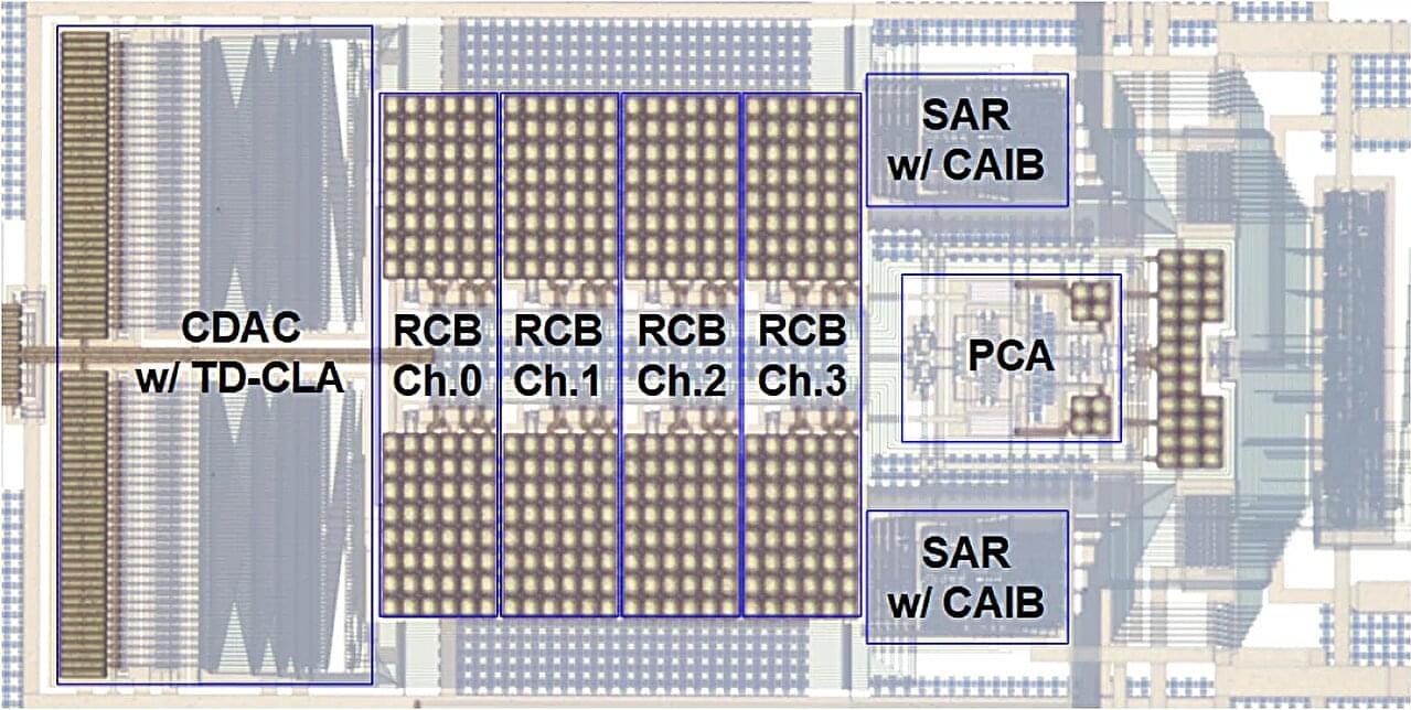
Discussions among regulators come as Beijing seeks to achieve self-sufficiency in semiconductor production.
Scientists have unveiled a technique that uses ‘molecular antennas’ to direct electrical energy into insulating nanoparticles. This approach creates a new family of ultra-pure near-infrared LEDs that could be used in medical diagnostics, optical communication systems, and sensitive detectors.
Researchers at the Cavendish Laboratory, University of Cambridge have discovered how to drive electrical current into materials that normally do not conduct, a feat previously thought impossible under normal conditions. By attaching carefully chosen organic molecules that act like tiny antennas, they have built the first light-emitting diodes (LEDs) from insulating nanoparticles. Their work, reported in Nature, points toward a new generation of devices for deep-tissue biomedical imaging and high-speed data transmission.
Integrated circuits are the brains behind modern electronic devices like computers or smart phones. Traditionally, these circuits—also known as chips—rely on electricity to process data. In recent years, scientists have turned their attention to photonic chips, which perform similar tasks using light instead of electricity to improve speed and energy efficiency.
Electrons can be elusive, but Cornell researchers using a new computational method can now account for where they go—or don’t go—in certain layered materials.
Physics and engineering researchers have confirmed that in certain quantum materials, known as “misfits” because their crystal structures don’t align perfectly—picture LEGOs where one layer has a square grid and the other a hexagonal grid—electrons mostly stay in their home layers.
This discovery, important for designing materials with quantum properties including superconductivity, overturns a long-standing assumption. For years, scientists believed that large shifts in energy bands in certain misfit materials meant electrons were physically moving from one layer to the other. But the Cornell researchers have found that chemical bonding between the mismatched layers causes electrons to rearrange in a way that increases the number of high-energy electrons, while few electrons move from one layer to the other.
In the next section, we’ll look at the ways scientists can grow nanowires from the bottom up.
Looking at the Nanoscale.
A nanoscientist’s microscope isn’t the same kind that you’ll find in a high school chemistry lab. When you get down to the atomic scale, you’re dealing with sizes that are actually smaller than the wavelength of visible light. Instead, a nanoscientist could use a scanning tunneling microscope or an atomic force microscope. Scanning tunneling microscopes use a weak electric current to probe the scanned material. Atomic force microscopes scan surfaces with an incredibly fine tip. Both microscopes send data to a computer, which assembles the information and projects it graphically onto a monitor.
Developing an advanced Brain-Computer Interface (BCI) is only the beginning.
“In order to prove a theory of consciousness is right, you have to see it for yourself,” Hodak explains. “That will require these big brain-computer interfaces.”
Hodak thinks that once humans understand how billions of neurons bind together to create a unified experience — what neuroscientists call “the binding problem” — we can start doing truly wild things.
I almost hesitate to say some of those wild things include multiple brains working to form one consciousness. “You could really, in a very fundamental sense, talk about redrawing the border around a brain, possibly to include four hemispheres, or a device, or a whole group of people,” he says.