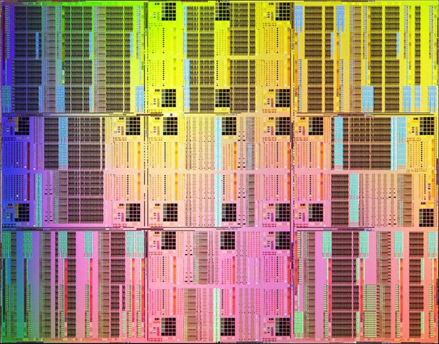
Moore’s Law might not be dead, but it is kinda zombified.


A new approach for identifying signs of hidden awareness in people who cannot speak or move after severe brain injury has been demonstrated by researchers at the University of Bath in the U.K.
The system detects patterns of brain activity through a wearable headset using an advanced application of brain-computer interface (BCI) technology.
Across multiple experimental sessions, the researchers uncovered signs of consciousness that were previously undetected in unresponsive patients.

A problem once touted as requiring a quantum computer has now been solved on a laptop.
Using advanced mathematical techniques and sophisticated software, physicists at the Center for Computational Quantum Physics (CCQ) at the Simons Foundation’s Flatiron Institute and collaborators at Boston University showed that a conventional computer can successfully simulate a notoriously difficult quantum system previously claimed to be beyond the reach of classical computing.
What if intelligence doesn’t require a brain? Biologist Michael Levin argues that intelligence is not confined to neurons, but exists on a continuum of goal-directed behavior and problem-solving across a wide range of species and systems. Using a framework he calls the “cognitive light cone,” Levin explores diverse forms of intelligence extending all the way down to the cellular level. His research suggests that cells communicate through electrical networks, enabling them to make collective decisions and adapt to unexpected challenges, evidenced by engineered tadpoles capable of seeing through eyes located on their tails. Levin radically challenges the conventional wisdom even further, proposing that forms of intelligence may extend beyond biology to molecular systems and maybe even the weather.
00:00 What is intelligence?
01:03 The field of diverse intelligence.
01:33 Intelligence at the cellular level.
02:08 The cognitive light cone.
03:01 The intelligence of groups of cells.
03:52 The bioelectric language of cells.
04:20 The mind of the body.
04:23 Cells that solve problems.
05:17 The tadpole experiment.
06:25 The cognitive spectrum.
06:48 Can you train a hurricane?
07:03 A new science of intelligence.
07:28 Beyond human biases.
——–
Quanta Magazine is an editorially independent publication supported by the Simons Foundation. We focus on developments in mathematics, theoretical physics, theoretical computer science and the basic life sciences.
READ free math and science articles on the Quanta website: https://www.quantamagazine.org.
LEARN about the Simons Foundation: www.simonsfoundation.org.
FOLLOW our social channels:
Materials called relaxor ferroelectrics have been used for decades in technologies like ultrasounds, microphones, and sonar systems. Their unique properties come from their atomic structure, but that structure has stubbornly eluded direct measurement.
Now a team of researchers from MIT and elsewhere has directly characterized the three-dimensional atomic structure of a relaxor ferroelectric for the first time. The findings, reported today in Science, provide a framework for refining models used to design next-generation computing, energy, and sensing devices.
“Now that we have a better understanding of exactly what’s going on, we can better predict and engineer the properties we want materials to achieve,” says corresponding author James LeBeau, MIT’s Kyocera Professor of Materials Science and Engineering. “The research community is still developing methods to engineer these materials, but in order to predict the properties those materials will have, you have to know if your model is right.”
Buy Anker Prime 160W Charger on US Amazon: https://ankerfast.club/AnkerTech_302069
Visit the official website to learn more about Ask Me Anker-Thing: https://shop.anker.com/AnkerTech_anas…
#AnkerTech.
Timestamps:
00:00 — New Semiconductor.
08:44 — Computers of The Future.
My Podcast on Apple: https://podcasts.apple.com/at/podcast…
My Podcast on Spotify: https://open.spotify.com/show/3drr7A8… Let’s connect on LinkedIn: / anastasiintech Newsletter: https://anastasiintech.substack.com Instagram:
/ anastasi.in.tech Patreon:
/ anastasiintech.
Let’s connect on LinkedIn: / anastasiintech.
Newsletter: https://anastasiintech.substack.com.
Instagram: / anastasi.in.tech.
Patreon: / anastasiintech.
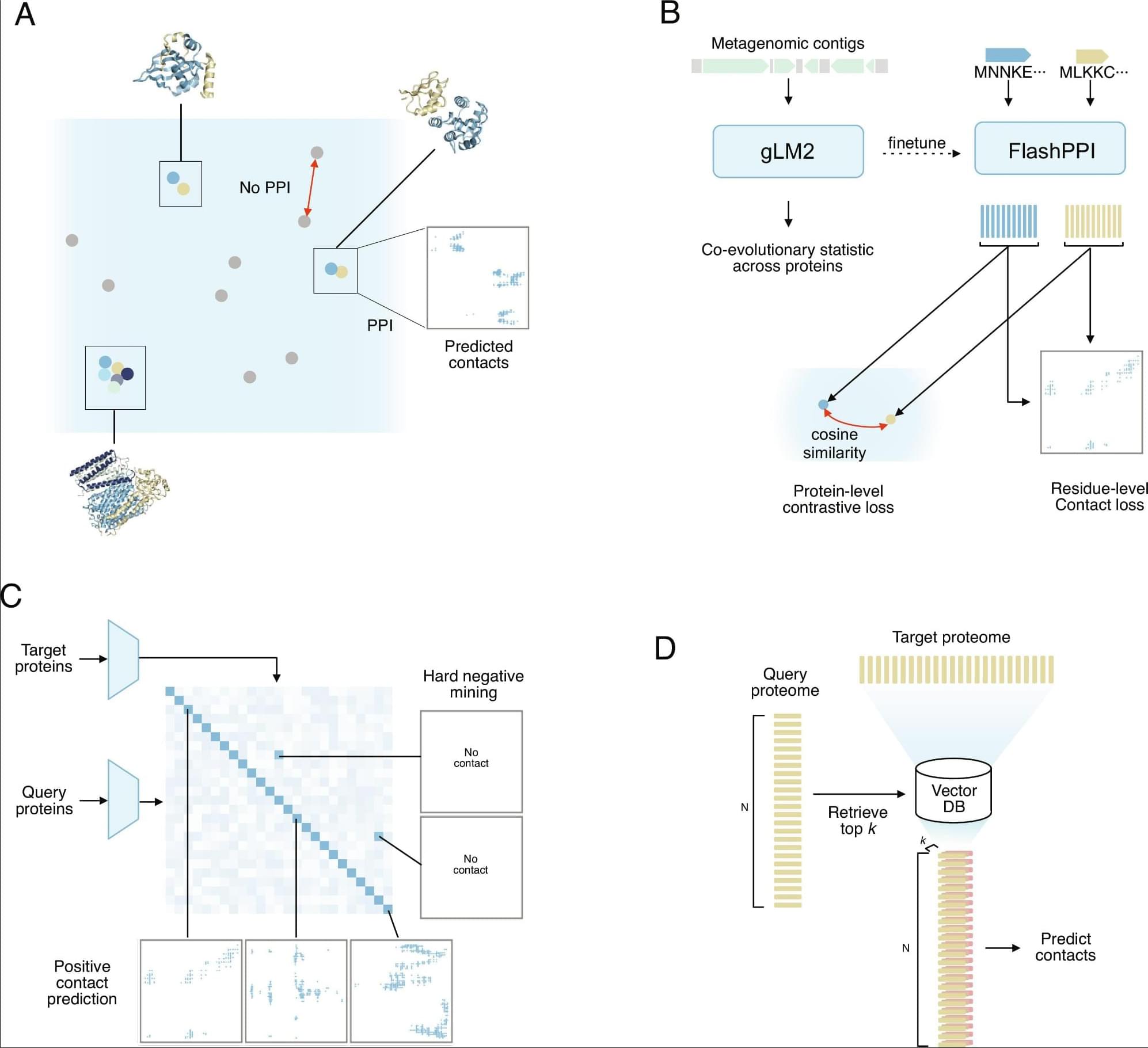
Protein–protein interactions (PPIs) underpin biological function, yet proteome-scale interaction prediction remains bottlenecked by the quadratic computational complexity of all-vs.-all pairwise comparisons. Here, we present FlashPPI, a contrastive learning framework, grounded in residue-level interactions, that enables linear-time prediction of physical protein interfaces across a microbial proteome. By leveraging a genomic language model that captures cross-protein coevolutionary signals from metagenomic sequences, FlashPPI aligns interacting partners in a shared latent space. We demonstrate a four-fold performance increase over existing sequence-based methods, while reducing proteome-wide screening time from days to minutes. Crucially, FlashPPI achieves comparable screening performance to state-of-the-art structure-folding models at a fraction of the computational cost. Finally, we integrate FlashPPI into an interactive web platform that combines predicted networks with functional annotations and genomic context, making proteome-wide network analysis rapid and accessible for microbial discovery.
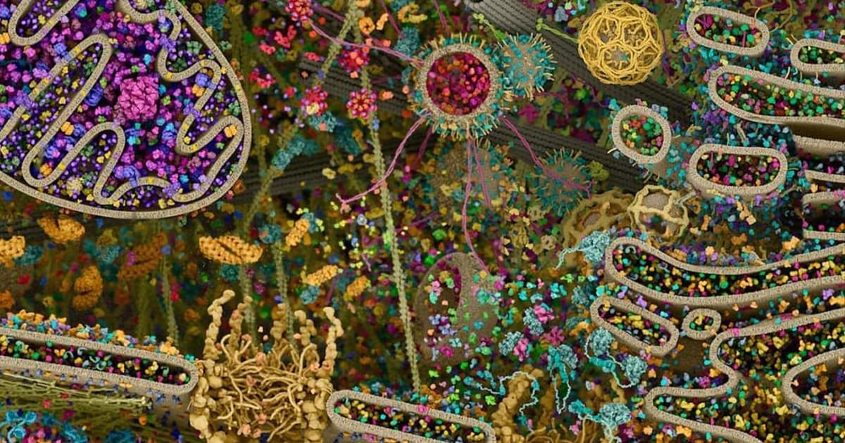
The interactive image was created for Cell Signaling Technology, Inc., and was inspired by the work of David Goodsell, a professor of computational biology at Scripps Research Institute, who is widely recognized for his vibrant watercolor paintings of cells and viruses. Alongside some artistic interpretation, portions of the image were digitally rendered using datasets gathered through scientific methods.
“This 3D rendering of a eukaryotic cell is modeled using X-ray, nuclear magnetic resonance (NMR), and cryo-electron microscopy datasets for all of its molecular actors,” explains McGill. “It is an attempt to recapitulate the myriad pathways involved in signal transduction, protein synthesis, endocytosis, vesicular transport, cell-cell adhesion, apoptosis, and other processes.”
Although some online are calling it “the most detailed image of a human cell ever captured” Evan Ingersoll and Gael McGill emphasize that it’s really an educational tool. Elements of the cell have been simplified, and in some cases “squashed together,” to help viewers better understand what happens inside it.