Toggle light / dark theme

Scientists Expose Hidden Quantum Identity of a Superconductor

Two strongly coupled superconducting states can disguise themselves as a single energy gap in ultrathin materials.

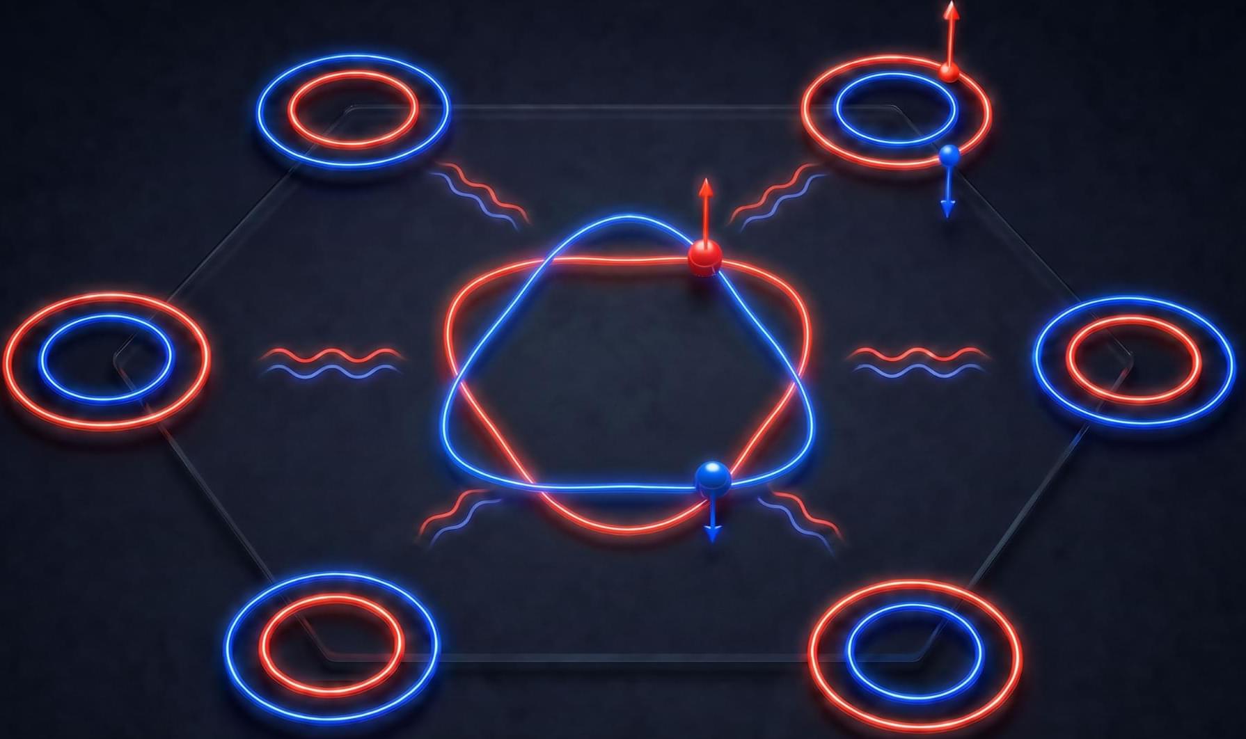
Two ultrathin superconductors appeared to have a simple internal structure, but closer measurements revealed something more complex. Instead of relying on one superconducting state, each material contains two strongly coupled states whose combined behavior makes them look like a single one.

The finding resolves a persistent mystery surrounding these materials and provides a more accurate picture of how their superconductivity works. That understanding could eventually help researchers develop improved materials for quantum computers, ultra-efficient electronics, advanced sensors, and other superconducting technologies.

A temperature dial for more realistic quantum simulations

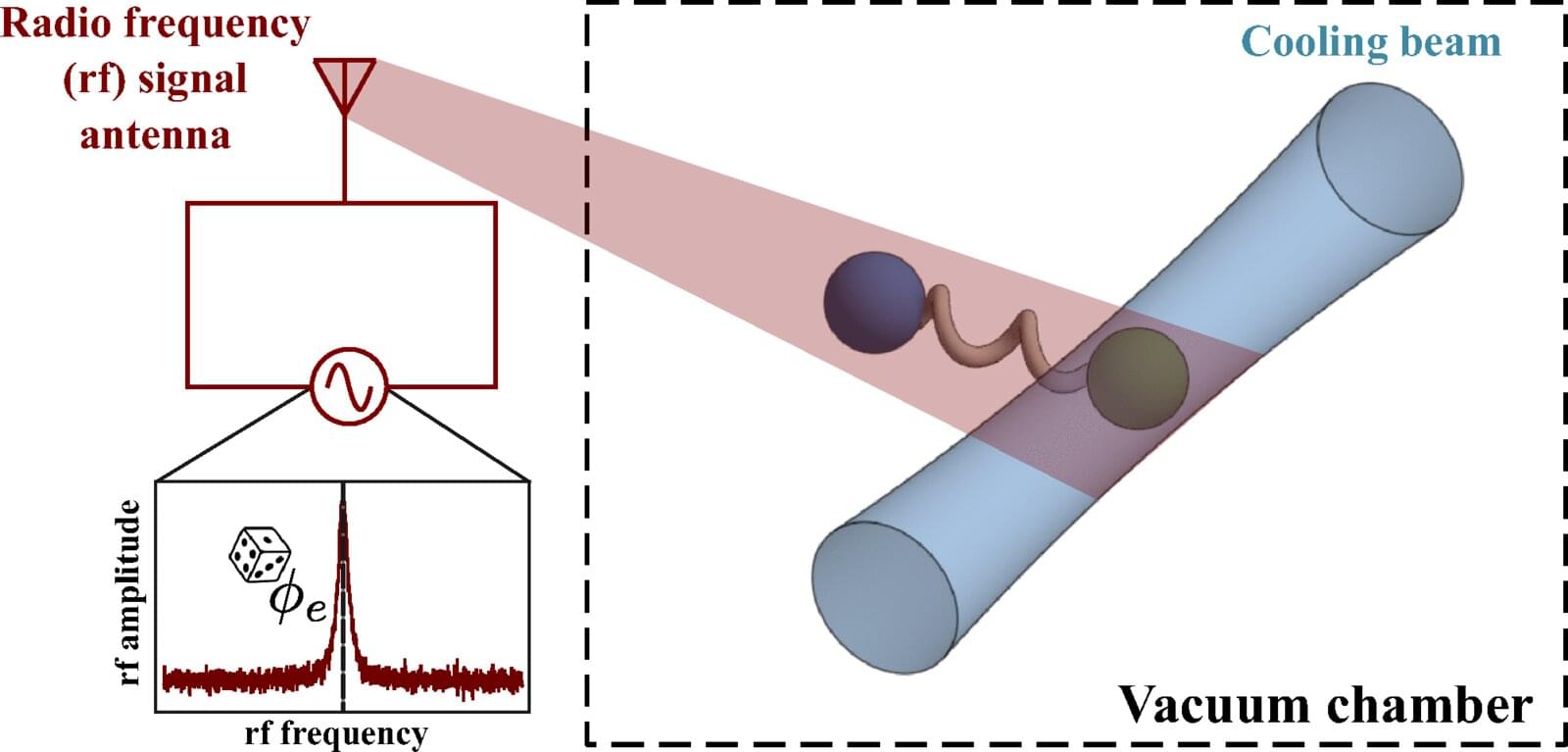
Scientists from Rice University in the U.S. have developed a way to precisely tune the temperature inside a trapped-ion simulator. The breakthrough means they will be able to run quantum simulations at precise temperatures that better reflect real-world conditions.

Trapped-ion simulators are quantum devices that isolate charged particles inside a sealed vacuum chamber, using electric fields to hold them in place. They mimic and study complex quantum systems, such as chemical reactions or exotic materials, that are too difficult for ordinary computers to calculate.

Temperatures inside these devices are typically kept as close as possible to absolute zero so that thermal motion does not disrupt calculations or cause errors. But researchers lacked a suitable way to set the temperature without accidentally changing how fast the system loses energy. This meant that studies were mostly stuck using absolute zero or uncontrolled high temperatures.

Quantum fluid reveals hidden states that can be switched with a magnetic field

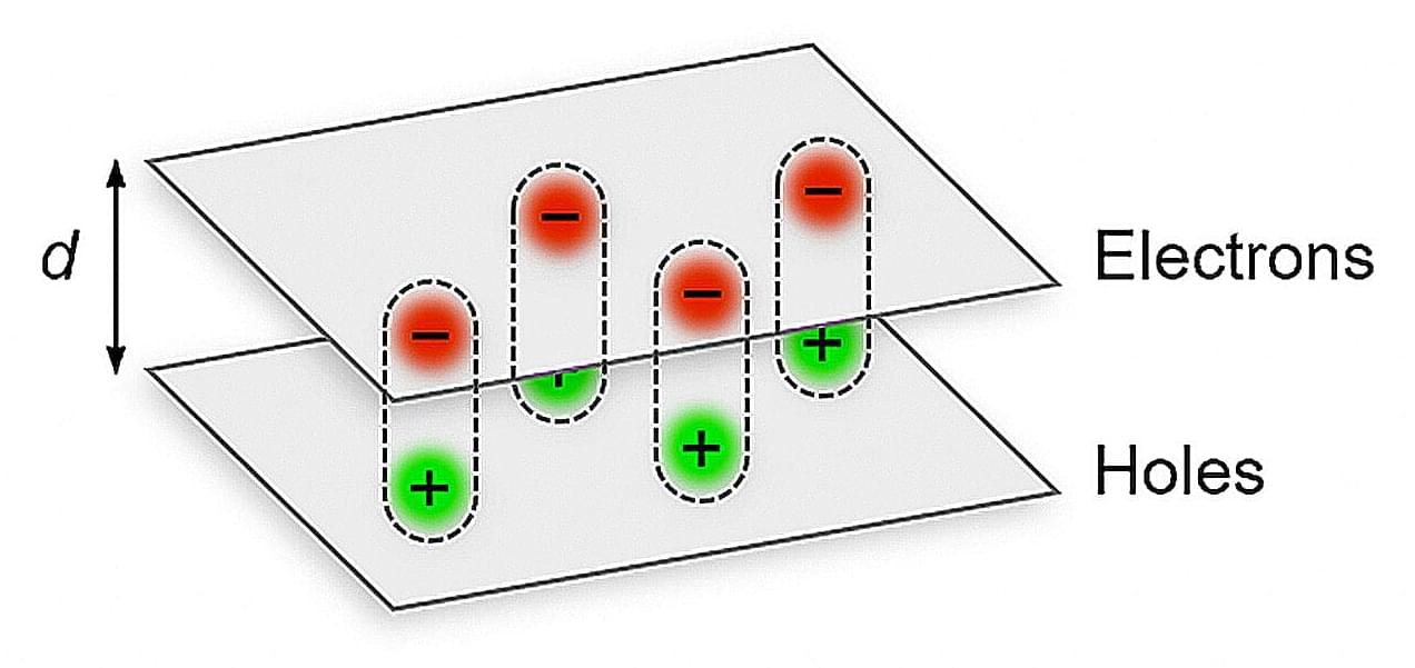
Bose-Einstein condensates (BECs) are often described as a “fifth state of matter”: a quantum state in which many particles lose their individual identities and behave as one collective object. For more than 60 years, researchers have sought to create such condensates from excitons—electron-hole pairs—as a solid-state route to macroscopic quantum coherence, which is useful for quantum technologies. This has been difficult to realize in controllable semiconductor devices because optically generated excitons have very short lifetimes of around a billionth of a second, and BECs are normally attained with ultracold gases in a vacuum.

But now, a team led by Lawrence Berkeley National Laboratory (Berkeley Lab) has observed a tunable BEC of excitons at high temperature in an atomically thin semiconductor. The findings, published in Nature, reveal not only that the excitons form a BEC but also that the condensate has an internal structure that can be switched by a magnetic field.

The work enables a new platform for studying quantum fluids in solid materials. (A quantum fluid is an exotic state of matter in which gases of electrons or other particles behave collectively like a fluid.) It also has implications for future quantum simulations, coherent optoelectronics in next-generation telecommunications and computing, and exciton-based devices enabling faster, more efficient computing.

Two materials, one photonic chip: Unlocking a new way to generate light frequencies

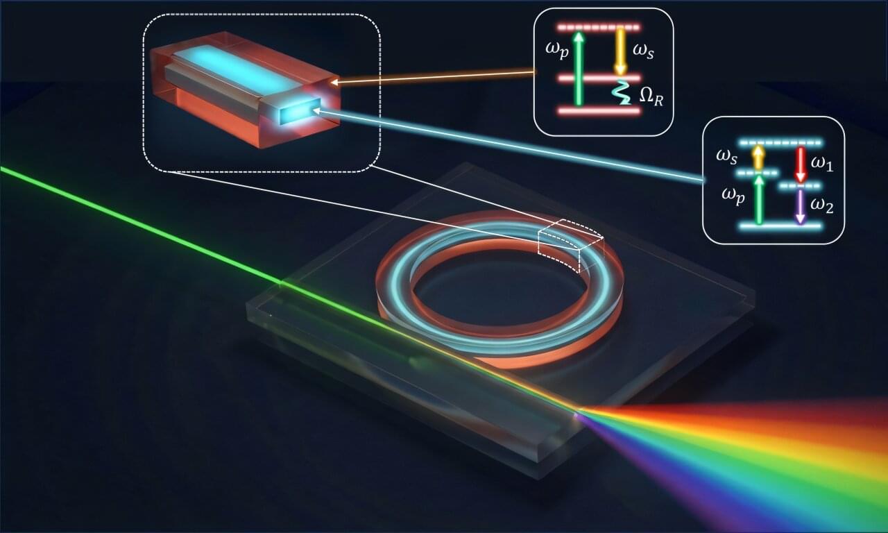
Modern photonic chips can pack sophisticated optical functions onto devices smaller than a fingernail. They are increasingly used to generate, manipulate and measure light for applications ranging from communications to sensing. But most of these chips rely on a single material to do the heavy lifting, limiting the range of optical effects they can produce.

Researchers have now demonstrated a different approach: letting two materials share the work. As reported in Advanced Photonics, scientists combined two nonlinear optical effects that normally occur separately. Their device uses a silicon nitride core to generate optical frequency combs while a surrounding silica layer produces Raman scattering.

By harnessing the strengths of both materials at once, the team created a new type of integrated photonic device capable of generating broad ranges of light frequencies on a chip.

Nano-optics: New mechanism for channeling light waves discovered in natural hyperbolic materials

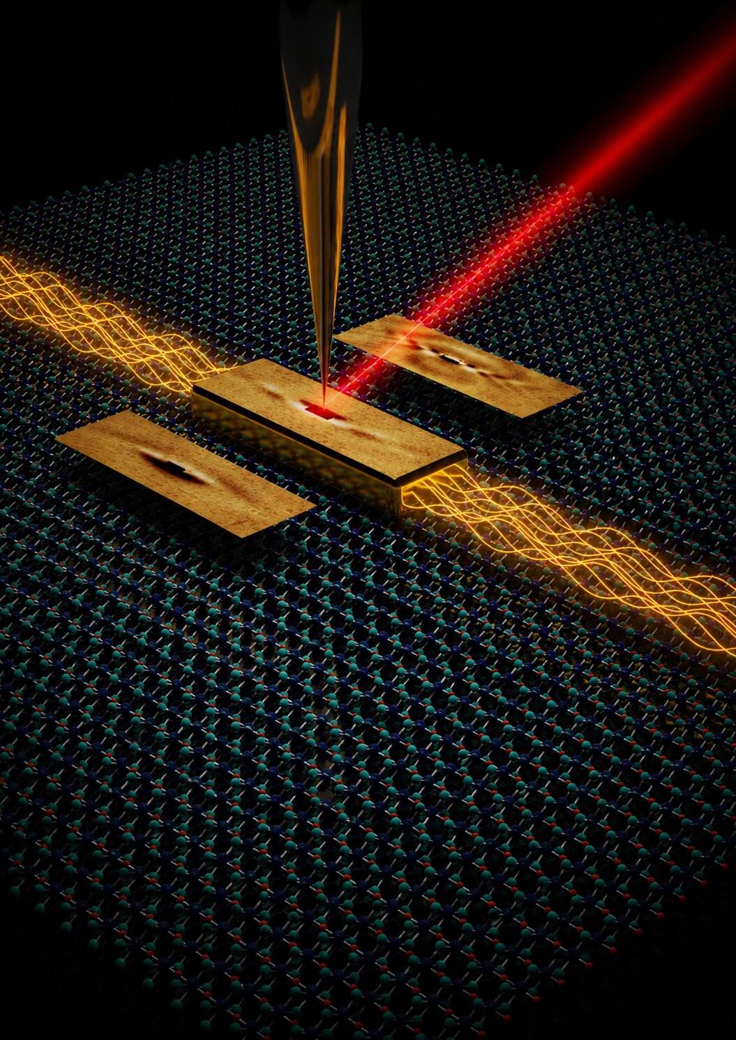
Researchers at the 4th Physics Institute of the University of Stuttgart and the Istituto Italiano di Tecnologia (IIT) in Milan have demonstrated a new mechanism for directing light in a naturally hyperbolic van der Waals material without conventional nanofabricated waveguides. The discovery opens new possibilities for integrated photonics, on-chip optical communication and future quantum technologies. The paper is published in the journal Nature Nanotechnology.

When a stone is dropped into water, circular waves spread outward from the point of impact. Light behaves similarly: When emitted from a localized source, it naturally propagates as spherical or circular wavefronts within a material. While this isotropic propagation is a fundamental property of waves, it is often undesirable in photonic applications where light must be guided efficiently along predefined paths.

Conventional optical technologies overcome this challenge using waveguides. In optical fiber communications, for example, glass fibers confine laser light and transport it over long distances with minimal loss. Similarly, photonic integrated circuits rely on nanoscale waveguides fabricated through complex lithographic processes, including resist coating, lithography and etching. These fabrication steps are technologically demanding and contribute significantly to manufacturing costs.

Lunar Ice Found Using Seismic Waves from Moonquakes

By simulating how moonquake vibrations travel faster through frozen soil, scientists developed a method using seismic waves to locate and measure buried water ice for future lunar missions. [ https://www.labroots.com/trending/space/30859/lunar-ice-foun…onquakes-2](https://www.labroots.com/trending/space/30859/lunar-ice-foun…onquakes-2)


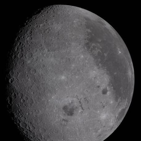
What new methods can be developed to identify locations of water ice on the Moon? This is what a recent study published in Science Advances hopes to address as a team of researchers investigated a novel method for identifying water ice deposits on the Moon. This study has the potential to help scientists, engineers, mission planners, and future astronauts use new strategies for finding lunar water ice, which could substantially reduce the financial and logistical costs of sending it from Earth.

For the study, the researchers used seismic waves produced by moonquakes to ascertain if these could be used to identify lunar water ice deposits. The primary motivation behind the study was to improve methods for identifying lunar water ice deposits, which comes as NASA is planning on returning humans to the Moon in 2028, along with ambitious plans to build a Moon base near the south pole.

To accomplish this study, the researchers used a combination of X-ray analysis of frozen volcanic rocks, computer simulations, and map analysis of the lunar south pole craters. In the end, the researchers found that lunar water ice stood out among lunar seismic waves, indicating this method could prove beneficial for future missions. The primary reason is the researchers found that lunar seismic waves move through water ice differently than dry regolith (aka Moon dust).
Turning molecules into reliable electronic devices with a new fabrication platform

Molecules are among the smallest building blocks available for making next-generation devices. Their unique, customizable properties enable promising applications in emerging computing, sensing, optical and quantum technologies.

But integrating molecules into functional devices at scale remains a challenge. Traditional semiconductor manufacturing processes can damage small, fragile molecular materials. Now, MIT researchers have developed a scalable fabrication technique that incorporates delicate molecular materials into electronic devices on a chip without causing damage.

Their method extends the capabilities of standard semiconductor manufacturing processes to accommodate molecules. The researchers first prefabricate the device components using traditional processes. Then, they introduce the molecules and harness nanoscale surface forces to mechanically transform the fabricated device, which self-assembles without damaging the molecules.

Pixel patterns harness diffraction for faster, more accurate nanoscale 3D printing

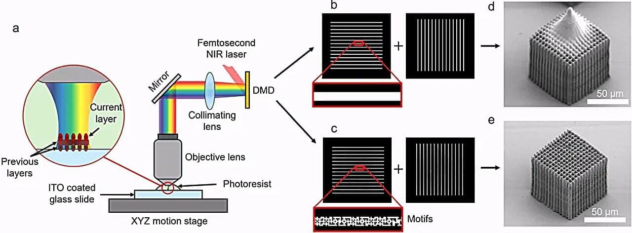
Researchers at the George W. Woodruff School of Mechanical Engineering have developed a new approach to nanoscale 3D printing that improves both speed and fidelity, overcoming a challenge that has limited the technology’s broader use in manufacturing.

Their work, led by Sourabh Saha, associate professor and Woodruff Faculty Fellow, and Harnjoo Kim, who conducted the research during his doctoral studies and later as a postdoctoral fellow in Saha’s lab, was recently published in the journal Nature Communications.

Nanoscale 3D printing allows researchers to create structures thousands of times smaller than the width of a human hair. These structures have potential applications in fields ranging from advanced computing and optics to biomedical devices and clean energy technologies. However, increasing printing speed often comes at the expense of quality.

Light controls nanoscale ‘bubble’ domains in a ferroelectric crystal

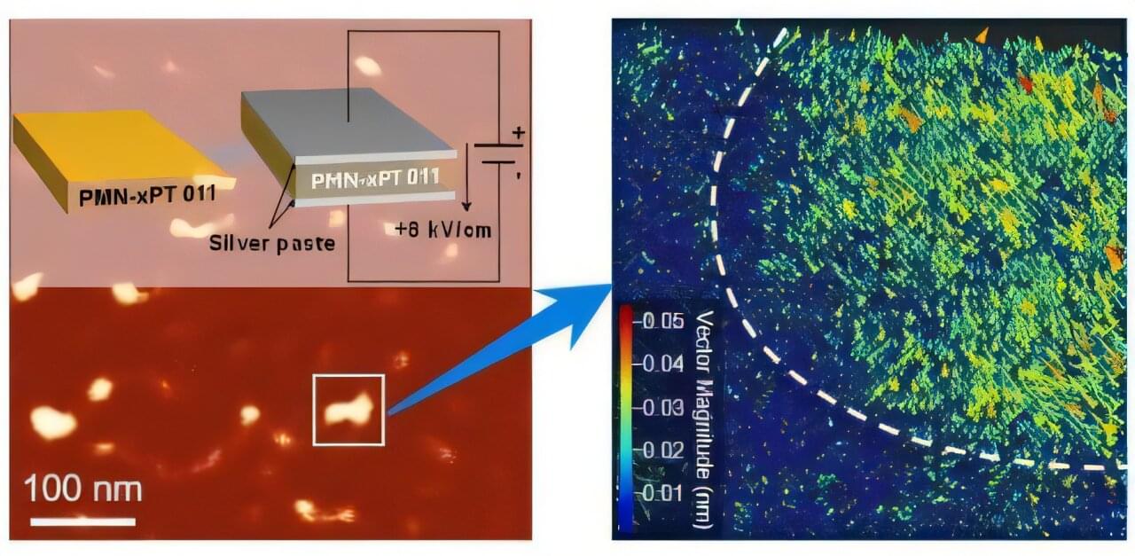
Researchers at Flinders University have discovered an unexpected way light can control tiny electronic structures inside advanced materials, a development that could help pave the way for more energy-efficient memory devices, sensors and future computing technologies.

The new study, involving experts from around the world, explores electronic properties and optical science to uncover new energy and material capabilities.

“We discovered that light can control nanoscale ‘bubble’ domains (about the size of just a few billionths of a meter across) inside a special ferroelectric crystal,” says Dr. Pankaj Sharma, senior lecturer in experimental condensed matter physics at Flinders University.

New quantum encryption method prevents ciphertext from being cloned

Digital security currently relies on difficult equations to protect data. For example, when you use a credit card online, the information is locked inside a math problem that would take a modern computer thousands of years to solve. However, if someone builds a powerful enough computer, that security breaks.

To make systems safer, there is a major shift toward quantum security. This is where the unbreakable laws of quantum physics can be used to protect data instead.

/* */