Now online! A scalable experimental and computational platform for mapping all organs and cell types in the mouse body, enabling comprehensive analysis of tissue organization and disease responses.


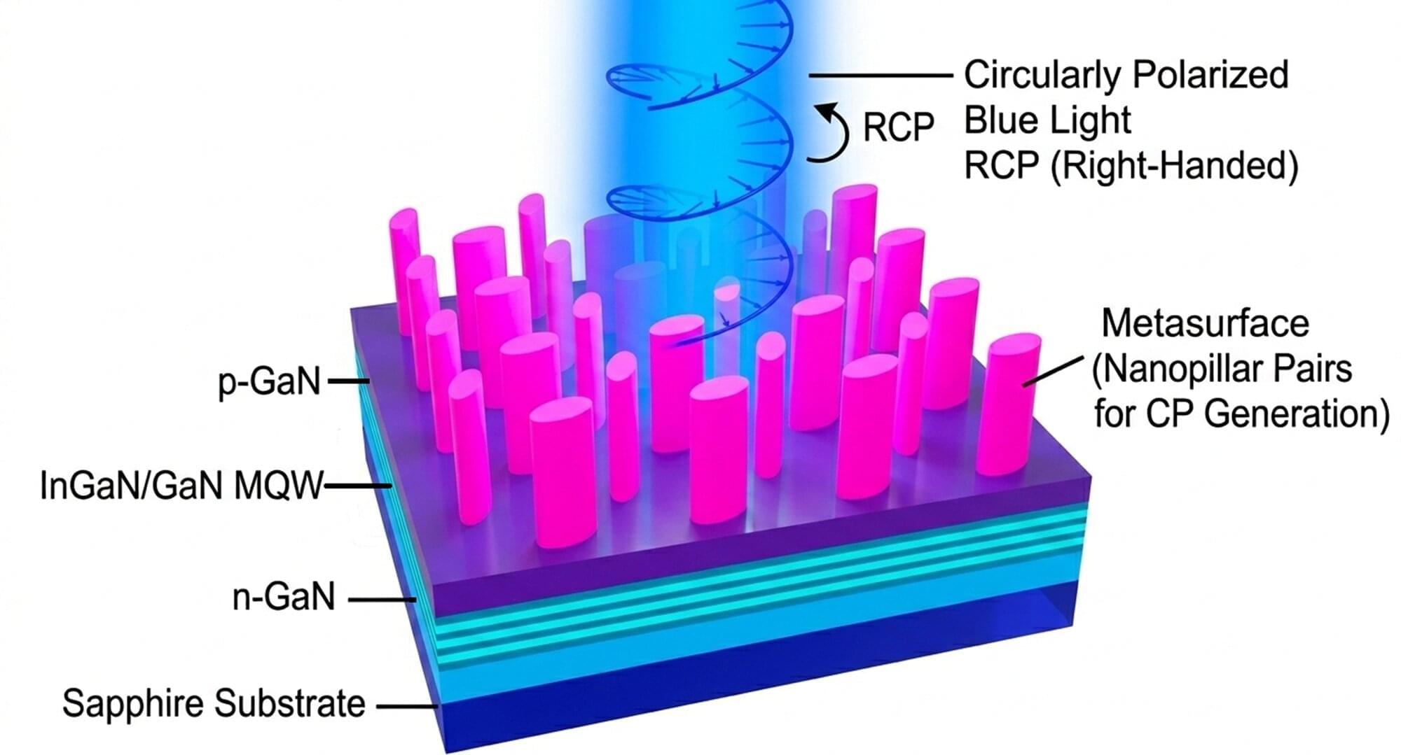
From 3D movie screens to augmented-reality devices, many modern technologies rely on our ability to manipulate light. Doing so in a cost-effective and efficient way, however, is often a formidable task. In an article published in Optics Letters, researchers from the University of Osaka announced a new light-emitting diode (LED) design that may help shrink complex optical systems into much smaller devices. The LED produces circularly polarized light using a built-in nanostructured surface, eliminating the need for bulky external optical components.
Circularly polarized light, whose electric field rotates like a corkscrew as it travels, is essential for technologies such as 3D displays, advanced imaging systems, and quantum communication tools. Traditionally, generating this kind of light requires optical components such as polarizers and special plates that modify the light’s phase. However, these components make devices larger, more complex, and harder to integrate.
“Our goal is to simplify the way circularly polarized light is produced,” says corresponding author Shuhei Ichikawa. “By integrating polarization control directly into the LED with a specially designed metasurface, we remove the need for additional optical components.”
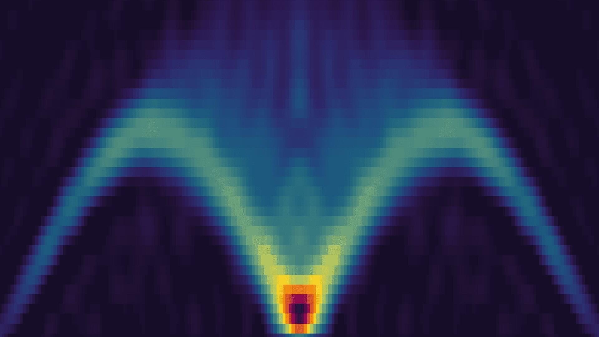
Studying and designing novel materials is a central application of quantum mechanics. Chemists, materials scientists, and physicists focus on subtle interactions in quantum materials and to uncover them they rely on sophisticated computational and experimental techniques. Computer simulations that connect microscopic quantum interactions to measurable material properties complement experimental data to connect structure to function—but classical computers can struggle to simulate those properties. Fortunately, scientists today have a new tool in their toolbox: quantum computers.
In new preprint, a team of researchers from Oak Ridge National Lab’s (ORNL’s) Quantum Science Center (QSC), Purdue University, Los Alamos Laboratory, the University of Illinois at Urbana-Champaign, the University of Tennessee, and IBM used quantum simulation to compute the energy-momentum spectrum of a well-studied magnetic material, KCuF3, showing strong agreement with the spectra measured via neutron scattering. The research is published on the arXiv preprint server.
The quantum simulations employed the IBM Quantum Heron processor, while the experimental data was acquired from neutron sources at the Spallation Neutron Source (SNS) at ORNL and at the Rutherford Appleton Laboratory in the United Kingdom. This work serves as another realization of Richard Feynman’s vision: the use of a well-controlled, programmable quantum system to simulate the properties of a quantum system of interest.
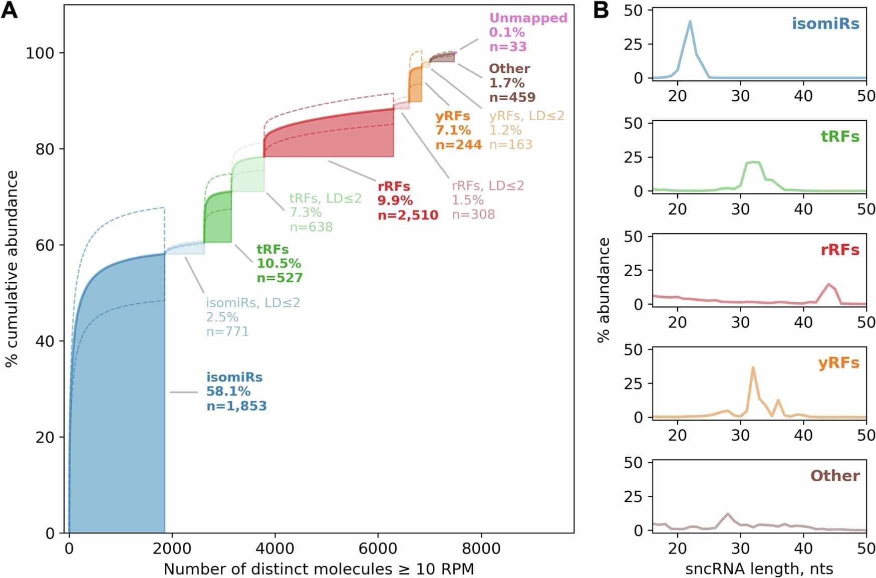
For decades, scientists studying brain disorders have focused almost exclusively on proteins and the genes encoding them. Now, research from Thomas Jefferson University’s Computational Medicine Center suggests that several classes of small regulatory molecules, fittingly known as small RNAs, may play a much larger role in schizophrenia and bipolar disorder, and in a healthy brain, than previously thought.
In a study recently published in Translational Psychiatry, a team led by Isidore Rigoutsos, Ph.D. took a comprehensive look at small RNAs in brain samples from people with schizophrenia, bipolar disorder and individuals without psychiatric illness. Their goal was to find out what kind of small RNAs are active in the brain, and whether their levels change in disease.
“Little attention had been paid to small RNAs in these disorders,” says Dr. Rigoutsos, “even though small RNAs help control numerous processes by modulating the abundance of genes.”

Researchers from Brown University and Mass General Brigham have developed an implantable brain-computer interface that allowed two people with paralysis — one with ALS and one with a spinal cord injury — to communicate through rapid, accurate typing. The system uses microelectrode sensors in the motor cortex, maps letters to attempted finger movements on a QWERTY keyboard, and decodes those neural signals into text.
In the study, one participant reached a top speed of 110 characters per minute (about 22 words per minute) with a 1.6% word error rate, and both participants were able to use the system from home after calibration with as few as 30 sentences. The results were published in Nature Neuroscience.
This is the kind of neurotechnology that starts to close the gap between thought and communication.
Implantable device research from the BrainGate clinical trial enables communication through rapid typing for a patient with ALS and a patient with a spinal cord injury.
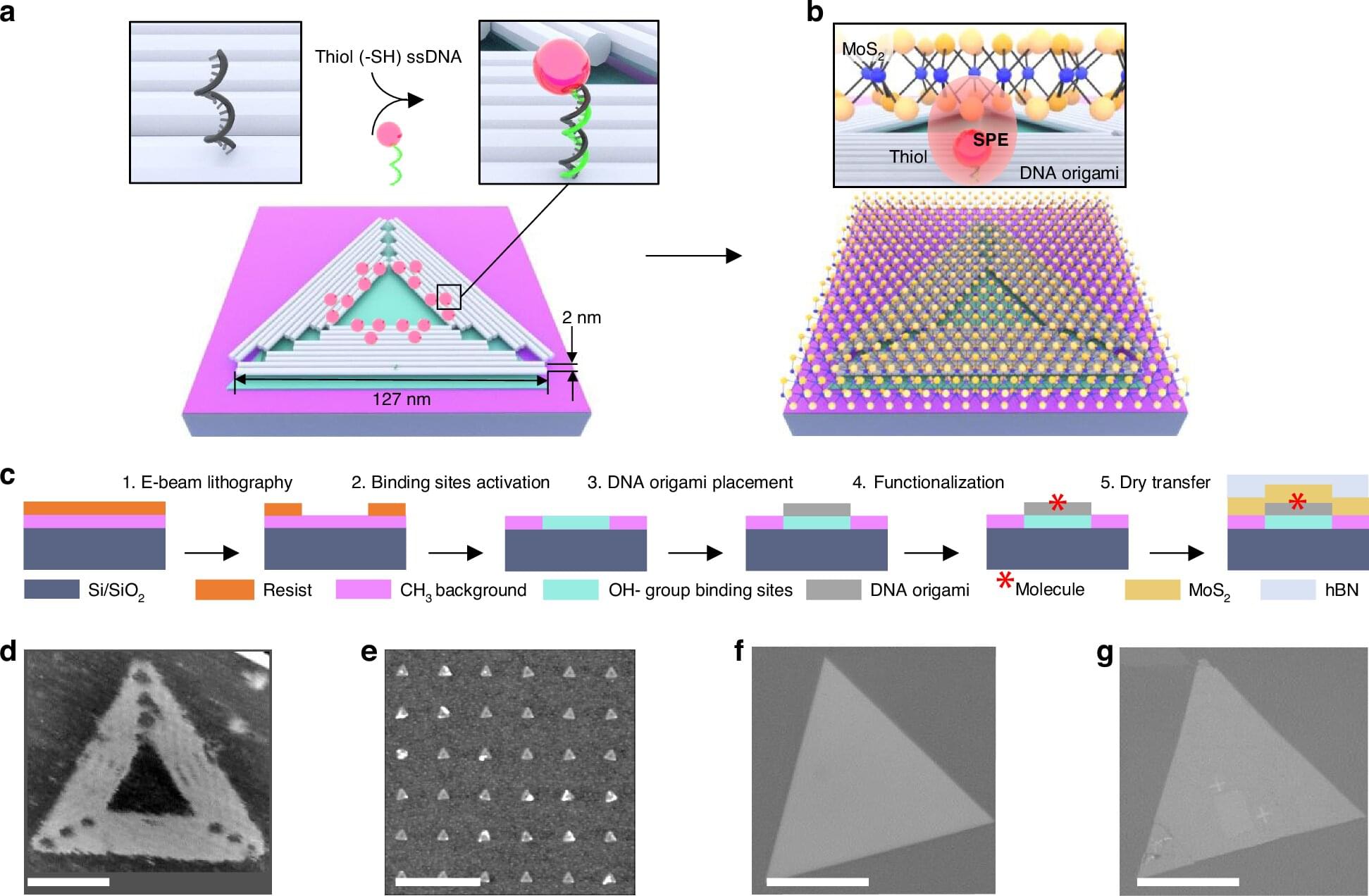
An international research team led by scientists from Skoltech has developed a method to position molecules on the surface of ultrathin materials with unprecedented precision using molecular DNA self-assembly, enabling the creation of quantum light sources. The results, published in the journal Light: Science & Applications, pave the way for the production of compact and efficient components for future quantum computers and secure communication networks.
Two-dimensional materials such as molybdenum disulfide are promising candidates for quantum light sources due to their ability to emit photons under laser excitation. However, until now, scientists have been unable to precisely control the location of emission centers—they emerged randomly upon ion beam irradiation or mechanical deformation of the material.
The authors of the study proposed a different approach. The research is based on the DNA origami method, which allows the construction of nanoscale objects of a specified shape from DNA molecules. Triangular structures measuring 127 nanometers were assembled, each carrying 18 thiol molecules. These structures were placed onto a silicon chip with a lithographic pattern. The positioning yield of each DNA origami structure at its designated location exceeded 90%, significantly surpassing the statistical limit of traditional single molecule deposition methods.

Caltech scientists have developed a new way to produce optical frequency combs—important tools in devices that keep time and measure distances very precisely—at the chip scale, an advance that should make it easier to incorporate such combs in optical devices and more practical to use them outside the laboratory.
To generate the combs, the new research demonstrates the utility of a robust class of light pulses, called topological solitons, that had been previously predicted but largely unexplored until now. The scientists, led by Caltech’s Alireza Marandi, professor of electrical engineering and applied physics, describe their findings in a paper published in Nature.
Frequency combs are light sources that emit a precise ruler-like “comb” of many evenly spaced frequencies. Over the last three decades, they have become important tools in spectroscopy, in telecommunications, and even in astronomical research. Currently, most frequency comb sources rely on bulky tabletop laser sources. The new work shows that an electrically pumped laser diode integrated with a photonic chip with strong nonlinearity can serve as a frequency comb source.

Phonons are the quantum units of mechanical vibration. They describe how motion propagates through a solid at the smallest possible scales, in much the same way that electrons describe electric currents. Because phonons can be exceptionally stable and sensitive, they are used in quantum science and technology.
Researchers can already detect and control individual phonons. The problem lies in making phonons interact with each other in a predictable and tunable way, which would be a key requirement for building complex quantum systems like quantum computers.
Interactions are essential in quantum technologies. Whether the goal is sensing tiny forces or processing information, one quantum excitation must be able to influence another. In practice, this requires nonlinearity, which means that adding one excitation changes how the system responds to the next, rather than each excitation behaving independently.
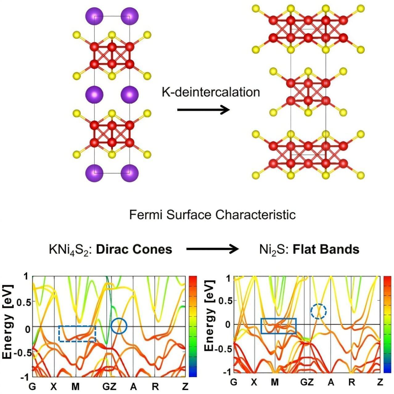
A team of scientists led by the U.S. Department of Energy’s (DOE) Argonne National Laboratory has identified a rare, switchable quantum property in a new type of nickel sulfide material. The discovery could have applications in high-speed transistors, adaptive sensors and other devices that require a material’s electronic structure to be controlled on the fly. The research is published in the journal Matter.
The compound, KxNi4S2 (0 ≤ x ≤ 1), contains nickel and sulfur sandwiched between layers of potassium. The “(0 ≤ x ≤ 1)” in the name means that the amount of potassium in the material can vary from no potassium at all to a full potassium atom, depending on the sample.
First detailed in a 2021 paper, it was created as part of an ongoing quest to develop more superconductors. As researchers examined the layered material’s characteristics, they happened upon a remarkable feature: applying an electrical current could drive the potassium layers out, collapsing the sandwich and changing the material’s structure.

Large-scale quantum computers are waiting in the wings. One of the main reasons we don’t have them yet is because quantum hardware is so noisy. This isn’t the type of noise you’d want to shush in a crowded theater. When it comes to computers, noise means errors that crop up when conditions aren’t perfect.
“We need to find a way to detect errors and correct for them,” said graduate student Evangelos Piliouras. Working with physicist Ed Barnes, Piliouras devised a method to reduce the noise and make quantum computers more noise tolerant. His work was published in npj Quantum Information.
Noise can have real-world implications even in a traditional computer, which uses a stream of electrical signals called bits that represent the 1s and 0s that make up binary code. Noise can knock a 0 into a 1, and a credit card transaction, for instance, might fail.