Malicious Packagist Laravel packages install a cross-platform RAT enabling remote shell access and system reconnaissance via C2 server.


Researchers at the University of Innsbruck, together with partners from Sydney and Waterloo, have presented a new diagnostic method for quantum computers. It makes errors in individual quantum bits visible during logical calculation and evaluates them. The new method was demonstrated on an ion trap quantum processor in Innsbruck. It can be used to identify critical error sources—a key to developing more robust, fault-tolerant quantum processors.
In Physical Review X, the researchers present a scalable method that can be used to reliably characterize logical quantum operations at the level of the underlying quantum bits. Cycle error reconstruction identifies which physical errors influence the performance of logically encoded gates.
“With cycle error reconstruction, we can quantitatively capture the error structure and clearly distinguish between correctable and uncorrectable contributions,” says first author Robert Freund from the Department of Experimental Physics.
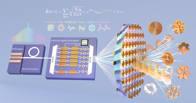
Using a chip-based microcomb, full dimensional control of structured microwaves is demonstrated, including vortex-microwave generation, submicrosecond spatiotemporal mode switching, broadband phase–frequency response tuning and wide-angle two-dimensional beam steering. These capabilities are applied in a structured-microwave-based integrated sensing and communication system.

“Our system provides a pathway towards a fast, scalable tool for measuring real-time brain activity in synthetic tissue cultures that replicate human brain tissue,” Associate Professor Simpson said.
If successful, this brain-on-chip technology could help evaluate the effectiveness of treatments for neurological diseases, including Alzheimer’s, schizophrenia, epilepsy and anxiety, in the laboratory before moving into expensive and complex human trials.
Cortical Labs hopes neuronal chips will do much more than shoot pixelated demons.

Something once thought too delicate for real cities just survived them. A quiet test in Germany hints that the next internet may be both unbreakable and already under our feet.
On a 30-kilometer loop of commercial fiber in Berlin, researchers just teleported data while ordinary internet traffic flowed on the same line without a hiccup. The feat, executed by T-Labs with Qunnect’s Carina platform, kept delicate quantum states steady against city vibrations and temperature swings, hitting 95 percent fidelity in real time. It shows that today’s networks can carry tomorrow’s quantum links, with stakes that range from unbreakable cryptography to connected quantum computers. For Deutsche Telekom’s Abdu Mudesir, it also signals a path to European technological sovereignty as the system scales to longer distances and more nodes.
Microscopy has long been essential to biomedical research, enabling detailed analyses of complex samples. Fourier ptychographic microscopy (FPM), a computational imaging technique, provides high-resolution, wide-field images without requiring extensive hardware modifications. However, current FPM algorithms struggle with samples exhibiting depth variations, such as tilted or 3-dimensional (3D) objects. The limited depth of field (DoF) leads to images with only focal-plane areas in sharp focus, while regions outside appear blurred. To address this limitation, we propose an all-in-focus FPM algorithm using physics-informed 3D neural representations to reconstruct sharp, wide-field images of 3D objects under limited DoF. Unlike previous methods, our approach samples the full depth range to create a 3D feature volume that incorporates spatial and depth information.

Neuromorphic engineering (NE) encompasses a diverse range of approaches to information processing that are inspired by neurobiological systems, and this feature distinguishes neuromorphic systems from conventional computing systems. The brain has evolved over billions of years to solve difficult engineering problems by using efficient, parallel, low-power computation. The goal of NE is to design systems capable of brain-like computation. Numerous large-scale neuromorphic projects have emerged recently. This interdisciplinary field was listed among the top 10 technology breakthroughs of 2014 by the MIT Technology Review and among the top 10 emerging technologies of 2015 by the World Economic Forum.