Download Opera for free using https://opr.as/Opera-browser-anastasiintech Thanks Opera for sponsoring this video!Timestamps:00:00 — Intro00:52 — Computing w…
Category: computing – Page 373
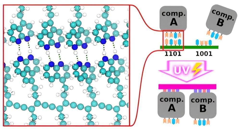
Research combines DNA origami and photolithography to move one step closer to molecular computers
Molecular computer components could represent a new IT revolution and help us create cheaper, faster, smaller, and more powerful computers. Yet researchers struggle to find ways to assemble them more reliably and efficiently.
To help achieve this, scientists from the Institute of Physics of the Czech Academy of Sciences investigated the possibilities of molecular machine self-assembly building upon solutions honed by natural evolution and using synergy with current chip manufacturing.
There is a limit to the miniaturization of current silicon-based computer chips. Molecular electronics, using single-molecule-sized switches and memories, could provide a revolution in the size, speed and capabilities of computers while cutting down on their increasing power consumption, but their mass production is a challenge. Large-scale, low-defect, accessible nanofabrication and assembly of the components remains elusive. Inspiration taken from living nature could change this status quo.
Using chaos to characterize a programmable analog quantum simulator
Adam Shaw (Caltech)https://simons.berkeley.edu/talks/adam-shaw-caltech-2024-04-23Near-Term Quantum Computers: Fault Tolerance + Benchmarking + Quantum Advant…
Researchers develop a new way to instruct dance in virtual reality
Researchers at Aalto University were looking for better ways to instruct dance choreography in virtual reality. The new WAVE technique they developed will be presented in May at the CHI conference for human-computer interaction research.
Previous techniques have largely relied on pre-rehearsal and simplification.
“In virtual reality, it is difficult to visualize and communicate how a dancer should move. The human body is so multi-dimensional, and it is difficult to take in rich data in real-time,” says Professor Perttu Hämäläinen.

Resurrection through simulation: questions of feasibility, desirability and some implications
Could a future superintelligence bring back the already dead? This discussion has come up a while back (and see the somewhat related); I’d like to resurrect the topic because … it’s potentially quite important.
Algorithmic resurrection is a possibility if we accept the same computational patternist view of identity that suggests cryonics and uploading will work. I see this as the only consistent view of my observations, but if you don’t buy this argument/belief set then the rest may not be relevant.
The general implementation idea is to run a forward simulation over some portion of earth’s history, constrained to enforce compliance with all recovered historical evidence. The historical evidence would consist mainly of all the scanned brains and the future internet.
‘Inspired by the human brain’: Intel debuts neuromorphic system that aims to mimic grey matter with a clear aim — making the machine exponentially faster and much more power efficient, just like us
Neuromorphic computing is about mimicking the human brain’s structure to deliver more efficient data processing, including faster speeds and higher accuracy, and it’s a hot topic right now. A lot of universities and tech firms are working on it, including scientists at Intel who have built the world’s largest “brain-based” computing system for Sandia National Laboratories in New Mexico.
Intel’s creation, called Hala Point, is only the size of a microwave, but boasts 1.15 billion artificial neurons. That’s a massive step up from the 50 million neuron capacity of its predecessor, Pohoiki Springs, which debuted four years ago. There’s a theme with Intel’s naming in case you were wondering – they’re locations in Hawaii.
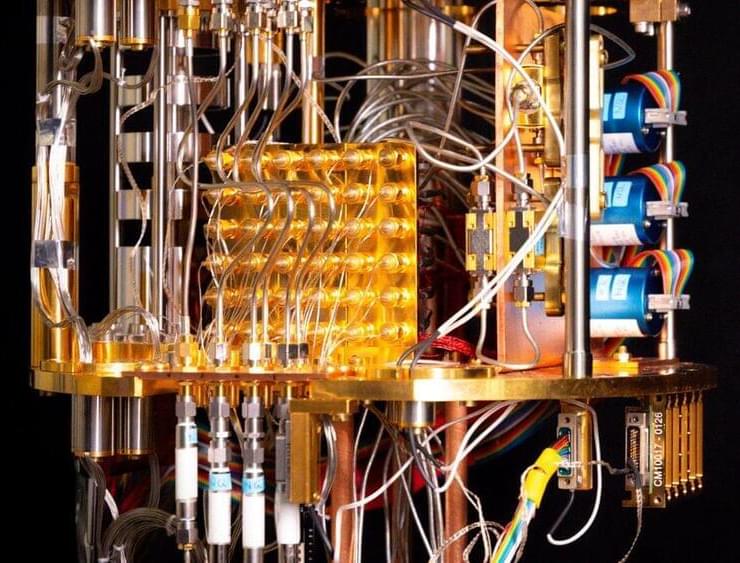
Bolometer measures state of superconducting qubit
For this technique to work at very high fidelity, a very fast and very sensitive bolometer is needed to measure the quantum state before it decays. In 2020, the Finnish researchers unveiled a bolometer that used graphene as its absorber – a fast and sensitive design that was intended for use in quantum computing. Unfortunately, this bolometer degraded over time and the team instead used an older bolometer design involving interfaces between superconductors and normal metals.
Möttönen says that the researchers had initially not expected the older design to be effective for reading out the states of individual qubits. He also expects that the read-out fidelity could be boosted using improved graphene bolometers. “I’m hoping to get the new graphene bolometers out of the oven soon,” he says.
David Pahl at the Massachusetts Institute of Technology believes that the work is very preliminary, but potentially very important. He says that the two most important performance metrics for a scheme to read out quantum states are the fidelity and the speed: “The state of the art speed that we’ve seen in the past year is 0.1 μs and 99.5% fidelity…[Möttönen and colleagues] showed 14 μs and 61.7%,” he says.
The Novel Material Revolutionizing Energy Storage
Washington University in St. Louis scientists have developed a novel material that supercharges innovation in electrostatic energy storage. The material is built from artificial heterostructures made of freestanding 2D and 3D membranes that have an energy density up to 19 times higher than commercially available capacitors.
Electrostatic capacitors play a crucial role in modern electronics. They enable ultrafast charging and discharging, providing energy storage and power for devices ranging from smartphones, laptops, and routers to medical devices, automotive electronics and industrial equipment. However, the ferroelectric materials used in capacitors have significant energy loss due to their material properties, making it difficult to provide high energy storage capability.
Quantum Breakthrough when Light makes Materials Magnetic
The potential of quantum technology is huge but is today largely limited to the extremely cold environments of laboratories. Now, researchers at Stockholm University, at the Nordic Institute for Theoretical Physics and at the Ca’ Foscari University of Venice have succeeded in demonstrating for the very first time how laser light can induce quantum behavior at room temperature — and make non-magnetic materials magnetic. The breakthrough is expected to pave the way for faster and more energy-efficient computers, information transfer and data storage.
Within a few decades, the advancement of quantum technology is expected to revolutionize several of society’s most important areas and pave the way for completely new technological possibilities in communication and energy.
Of particular interest for researchers in the field are the peculiar and bizarre properties of quantum particles — which deviate completely from the laws of classical physics and can make materials magnetic or superconducting.