Making a strange state of matter called a time crystal inside a quantum computer helped researchers stabilise a fragile quantum state inspired by Schrödinger’s cat.


Making a strange state of matter called a time crystal inside a quantum computer helped researchers stabilise a fragile quantum state inspired by Schrödinger’s cat.

To show one of the advantages of being a cyborg, I typed my old prescription into ZEISS Optical Inserts which are for use with the Apple Vision Pro and it said “We are really sorry, but your prescription values go beyond the available range.”
But now that I’m a cyborg with artificial lenses, any optical inserts that I might need are very common and available.
Oh, I experimented a little and it looks like they can’t make lenses for −9.75 diopters or worse. My left-eye used to be −17.25!
We need your eyeglass prescription to create your ZEISS Optical Inserts – Prescription (sometimes also called distance prescription). This is why we ask you to upload it.
Contact lens prescriptions or ones for task-specific uses (office or computer glasses, near reading glasses) don’t qualify.

Hong-Ou-Mandel interference of single-#photon-level pulses stored in independent room-temperature #quantum #memories Quantum #repeater #networks require independent absorptive quantum memories capable of #storing and #retrieving indistinguishable photons to perform high-repetition entanglement…
Research with quantum computing and quantum networks is taking place around the world in the hopes of developing a quantum internet in the future. A quantum internet would be a network of quantum computers, sensors, and communication devices that will create, process, and transmit quantum states and entanglement and is anticipated to enhance society’s internet system and provide certain services and securities that the current internet does not have.
A team of Stony Brook University physicists and their collaborators have taken a significant step toward the building of a quantum internet testbed by demonstrating a foundational quantum network measurement that employs room-temperature quantum memories. Their findings are described in a paper published in npj Quantum Information.
The field of quantum information essentially combines aspects of physics, mathematics, and classical computing to use quantum mechanics to solve complex problems much faster than classical computing and to transmit information in an unhackable manner.
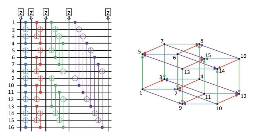
Despite the Harvard 48 logical #qubits paper is perhaps the biggest leap in #quantum technologies, still the final circuit is classically simulable.
Politics makes strange bedfellows, apparently so does quantum benchmarking.
In a surprising development, IBM Quantum and IonQ researchers teamed up to reveal an alternative classical simulation algorithm for an impressive error correction study conducted by a Harvard and QuEra team and published recently in Nature. IBM is a leader in superconducting quantum computers, while IonQ is noted as a pioneer in trapped ion devices.
The IBM-IonQ team reports in ArXiv that their classical algorithm accomplished the same computational task that was performed by the 48-qubit quantum setup in that Nature study, in a mere 0.00257947 seconds.

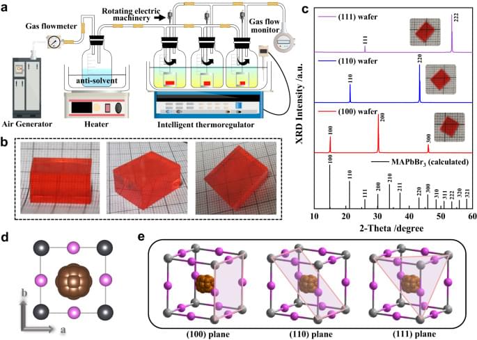
Based on the differently oriented MAPbBr3 single-crystal wafers, this study presents innovative findings primarily in two aspects. First, utilizing polarization-dependent ultrafast time-resolved spectroscopy, the anisotropic dynamics of photoexcited carriers on the picosecond timescale was first revealed. This discovery provides a deeper understanding of the ultrafast carrier relaxation pathways from the perspective of crystal orientation. It holds significant implications for exploring and expanding the potential of perovskite single crystals in polarization-sensitive and ultrafast optoelectronics applications, such as optical modulators, high-speed light polarization sensors, and ballistic transistors, which require both polarization sensitivity and high-field running capability simultaneously. However, a comprehensive understanding to correlate the observed polarization-dependent dynamics with the crystallographic structures has not been achieved yet due to limitations in current excited-state experimental techniques. Further progress will rely on employing more advanced ultrafast probing techniques, in combination with theoretical simulations, to comprehensively elucidate the observed carrier dynamics behind the underlying excited structure.
Second, by employing femtosecond laser processing, luminescent patterns with a remarkable three-order-of-magnitude PL enhancement on the bulk single crystals were achieved. The observed enhancement can be ultimately attributed to the synergy of three factors: the limited carrier diffusion length, the increase in shallow trap-assisted recombination centers, and the passivation of deep traps within the femtosecond laser-induced tentacle-like microstructures. In addition to offering a convenient top-down strategy for enhancing the photoluminescence intensity of bulk crystals, this study has also provided an in-depth understanding of the luminescence mechanism from multiple spatial (bulk and micro/nanoscale) and temporal (steady and transient-state) dimensions.


Dr. Janice Brahney: “Only recently have we started to see troubling outbreaks of toxic algal blooms in mountain environments. So, these changes are happening fast and are really concerning. It’s important we get to the bottom of this.”
What impact does atmospheric dust have on algae? This is what a recent study published in Global Change Biology hopes to address as a team of researchers from Utah State University (USU) investigated how increased dust concentrations in the Earth’s atmosphere could lead to larger algae blooms, impacting life on both land and in the oceans. This study holds the potential to help scientists better understand the acceptable amounts of dust and algae on the Earth and their impact on aquatic life, specifically in mountain ranges across the globe. The reason mountain headwater regions were the focus of the study was because they provide approximately 50% of the world’s population with fresh water.
“Only recently have we started to see troubling outbreaks of toxic algal blooms in mountain environments,” said Dr. Janice Brahney, who is an associate professor in the Watershed Sciences Department at USU and a co-author on the study. “So, these changes are happening fast and are really concerning. It’s important we get to the bottom of this. Toxic blooms in mountain lakes like the ones we’ve seen recently in remote mountain lakes are unprecedented.”
For the study, the researchers compared algae blooms and supplemented this with computer models to ascertain how atmospheric dust raining down onto the planet could impact aquatic communities, specifically with mountainous regions across the globe. In the end, the researchers found that increased atmospheric dust deposits not only increase algae populations, but also increase their tolerances for increased temperatures and pH, which are considered significant climate change factors.
