In a future with more ‘mind reading,’ thanks to computer-brain interfaces, we may need to rethink freedom of thought.
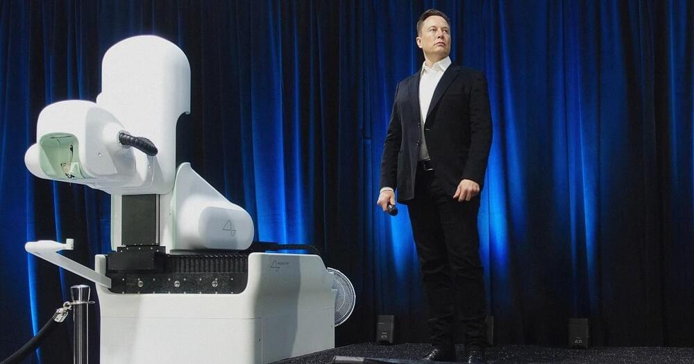


Scaling up qubit counts in quantum computers is at the core of achieving quantum supremacy.
Among the troublesome hurdles of this scaling-up race is refining how qubits are measured. Devices called parametric amplifiers are traditionally used to do these measurements. But as the name suggests, the device amplifies weak signals picked up from the qubits to conduct the readout, which causes unwanted noise and can lead to decoherence of the qubits if not protected by additional large components. More importantly, the bulky size of the amplification chain becomes technically challenging to work around as qubit counts increase in size-limited refrigerators.
Cue the Aalto University research group Quantum Computing and Devices (QCD). They have a hefty track record of showing how thermal bolometers can be used as ultrasensitive detectors, and they just demonstrated in an April 10 Nature Electronics paper that bolometer measurements can be accurate enough for single-shot qubit readout.

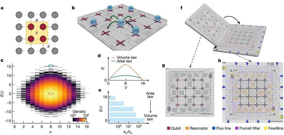
Entanglement is a form of correlation between quantum objects, such as particles at the atomic scale. The laws of classical physics cannot explain this uniquely quantum phenomenon, yet it is one of the properties that explain the macroscopic behavior of quantum systems.
Because entanglement is central to the way quantum systems work, understanding it better could give scientists a deeper sense of how information is stored and processed efficiently in such systems.
Qubits, or quantum bits, are the building blocks of a quantum computer. However, it is extremely difficult to make specific entangled states in many-qubit systems, let alone investigate them. There are also a variety of entangled states, and telling them apart can be challenging.
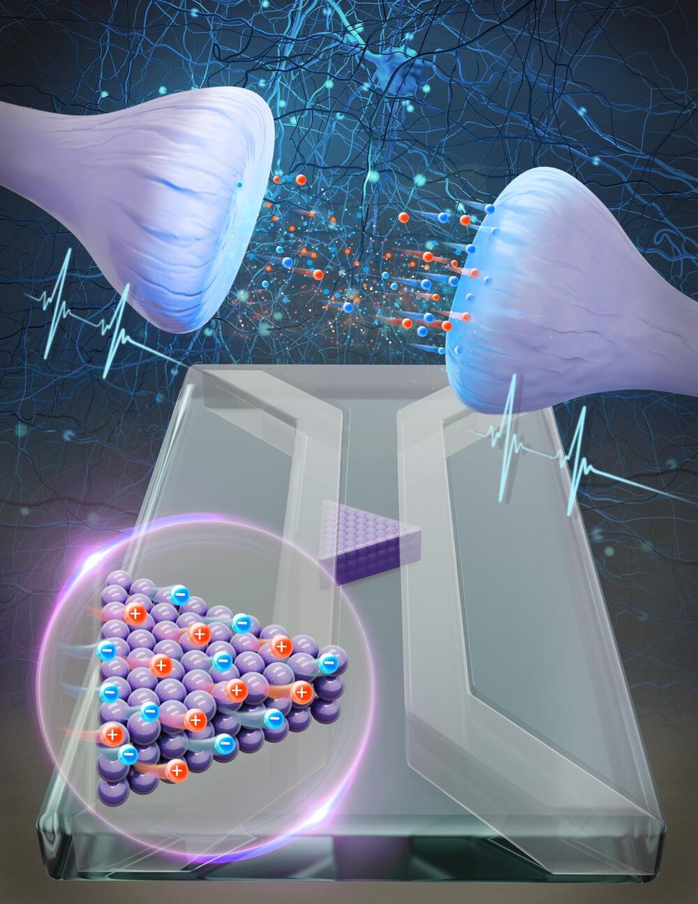
Theoretical physicists at Utrecht University, together with experimental physicists at Sogang University in South Korea, have succeeded in building an artificial synapse. This synapse works with water and salt and provides the first evidence that a system using the same medium as our brains can process complex information.
The results appear in the journal Proceedings of the National Academy of Sciences.
In the pursuit of enhancing the energy efficiency of conventional computers, scientists have long turned to the human brain for inspiration. They aim to emulate its extraordinary capacity in various ways.
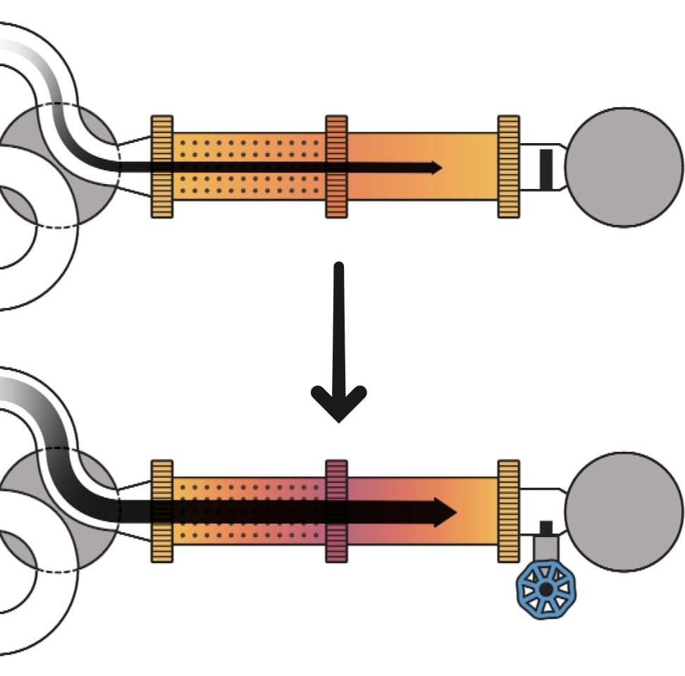
From stabilizing qubits (the basic unit of information in a quantum computer) to maintaining the superconducting properties of materials and keeping NASA’s James Webb Space Telescope cool enough to observe the heavens, ultracold refrigeration is essential to the operation of many devices and sensors. For decades, the pulse tube refrigerator (PTR) has been the workhorse device for achieving temperatures as cold as the vacuum of outer space.
These refrigerators cyclically compress (heat) and expand (cool) high pressure helium gas to achieve the “Big Chill,” broadly analogous to the way a household refrigerator uses the transformation of freon from liquid to vapor to remove heat. For more than 40 years, the PTR has proven its reliability, but it is also power-hungry, consuming more electricity than any other component of an ultralow temperature experiment.
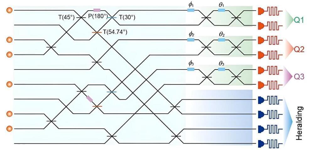
Photonic quantum computers are computational tools that leverage quantum physics and utilize particles of light (i.e., photons) as units of information processing. These computers could eventually outperform conventional quantum computers in terms of speed, while also transmitting information across longer distances.
Despite their promise, photonic quantum computers have not yet reached the desired results, partly due to the inherently weak interactions between individual photons. In a paper published in Physical Review Letters, researchers at University of Science and Technology of China demonstrated a large cluster state that could facilitate quantum computation in a photonic system, namely three-photon entanglement.
“Photonic quantum computing holds promise due to its operational advantages at room temperature and minimal decoherence,” Hui Wang, co-author of the paper, told Phys.org.
Check out courses in science, mathematics, or computer science on Brilliant! First 30 days are free and 20% off the annual premium subscription when you use our link ➜ https://brilliant.org/sabine.
The Future of Humanity Institute announced last week that they have shut down. Located at the University of Oxford in the UK prior to its demise, the institute was one of the few places worldwide studying the risk of human extinction and a few other controversial research areas. Let’s have a look at the events leading to the institute’s closure.
🤓 Check out my new quiz app ➜ http://quizwithit.com/
💌 Support me on Donorbox ➜ https://donorbox.org/swtg.
📝 Transcripts and written news on Substack ➜ https://sciencewtg.substack.com/
👉 Transcript with links to references on Patreon ➜ / sabine.
📩 Free weekly science newsletter ➜ https://sabinehossenfelder.com/newsle…
👂 Audio only podcast ➜ https://open.spotify.com/show/0MkNfXl…
🔗 Join this channel to get access to perks ➜
/ @sabinehossenfelder.
🖼️ On instagram ➜ / sciencewtg.
#science #sciencenews #FHI

How can we guarantee that data sent over the internet is only accessible to its intended recipient? Currently, our data is secured using encryption methods based on the premise that factoring large numbers is a complex task. However, as quantum computing advances, these encryption techniques may become vulnerable and potentially ineffective in the future.
Encryption by means of physical laws
Tobias Vogl, a professor of Quantum Communication Systems Engineering, is working on an encryption process that relies on principles of physics. “Security will be based on the information being encoded into individual light particles and then transmitted. The laws of physics do not permit this information to be extracted or copied. When the information is intercepted, the light particles change their characteristics. Because we can measure these state changes, any attempt to intercept the transmitted data will be recognized immediately, regardless of future advances in technology,” says Tobias Vogl.

A new project unites world-leading experts in quantum computing and genomics to develop new methods and algorithms to process biological data.
Researchers aim to harness quantum computing to speed up genomics, enhancing our understanding of DNA and driving advancements in personalized medicine
A new collaboration has formed, uniting a world-leading interdisciplinary team with skills across quantum computing, genomics, and advanced algorithms. They aim to tackle one of the most challenging computational problems in genomic science: building, augmenting, and analyzing pangenomic datasets for large population samples. Their project sits at the frontiers of research in both biomedical science and quantum computing.