Toggle light / dark theme

Ramped fields create more robust entanglement between trapped-ion qubits

While quantum computing could be the future, it is currently plagued by finicky hardware. To make the technology practical, researchers must demonstrate that it consistently and continuously works and performs at scale. In a new study, published in Physical Review Letters, researchers at Lawrence Livermore National Laboratory (LLNL) and the Ion Storage Group at the National Institute of Standards and Technology in Boulder, Colorado, created a robust process for entangling trapped-ion qubits. The result means better building blocks for ion-based quantum computers.

The approach creates a physical link between two trapped ions. Those ions are held in place with an electric field, although they do vibrate naturally. Because they have the same charge, they also repel each other. If one ion moves, it nudges its neighbor.

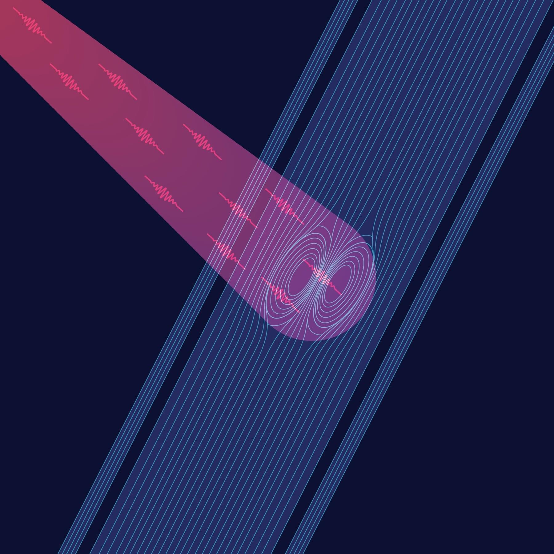
That shared motion can be used as a messenger between the qubits. In this experiment, the team used radio-frequency and microwave electromagnetic fields to apply a force to the ions. In different quantum states—say, when the qubit is pointing up versus down—the force pushes the shared-ion motion in a slightly different way.

Sound waves do double duty, carrying and protecting quantum information

Researchers at the Harvard John A. Paulson School of Engineering and Applied Sciences (SEAS) have demonstrated a promising new way to protect fragile quantum information using nothing but mechanical vibrations—essentially extremely small sound waves. The breakthrough, which comes from the lab of Marko Lončar, Tiantsai Lin Professor of Electrical Engineering, paves a path toward compact, sound-based quantum networks on chips, as well as hybrid quantum systems that combine many different types of quantum bits, or qubits.

The research is published in Nature Physics. Experiments were led by Eliza Cornell, a recent Ph.D. graduate from the Lončar lab and current postdoctoral researcher at Boston University, and Zhujing Xu, a former postdoctoral scholar in Lončar’s group.

Erasable semiconductor is programmed with light

Researchers at Princeton Engineering have created a semiconductor with unique properties: It is just a few molecules thick and can repeatedly change its properties in response to light. This is a step toward building more energy-efficient sensors, optoelectronic devices and computing technologies.

Advances in semiconductors over the past 50 years have allowed engineers to create increasingly smaller semiconductor devices and more efficient computers. But this approach is reaching its physical limits—the semiconductor devices are so tiny that it is challenging to add more devices. Researchers are now creating new materials rather than shrinking existing ones.

“One of the future goals for advancing electronics is not just making materials smaller, but making them adaptable and smarter,” said Jaehoon Ji, a postdoctoral researcher and first author on the July 1 paper describing the research in Science Advances.

Exact calculations sharpen view of atomic nuclei

Every high-energy nuclear collision leaves behind a trail of clues about the structure of atomic nuclei. Deciphering those clues, however, depends on the accuracy of the underlying theory. Physicists at Osaka Metropolitan University have now performed a full calculation within Glauber theory, a cornerstone framework for describing high-energy nuclear collisions.

By overcoming a computational challenge that has long forced researchers to rely on approximations to reduce computational demands, the team has shown that its full calculation can accurately reproduce experimental data and provide a reliable framework for predicting the outcomes of future experiments involving ordinary and exotic nuclei.

The study was published in Physical Review Letters on May 18 and Physical Review C on June 1. Physical Review Letters provides a brief overview of the main findings, while Physical Review C contains the complete paper with additional details, results and analysis.

Bright ideas accelerate the hunt for quantum emitters

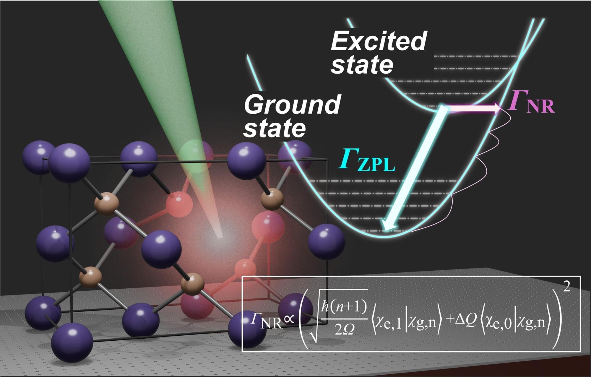
The search for materials that can power future quantum technologies is accelerating, but identifying the most promising candidates remains painfully slow. Evaluating whether a material can efficiently emit quantum light requires computationally intensive simulations, making it difficult to screen the vast number of available materials.

Now, researchers from the University of Osaka have overcome this bottleneck with a prediction method that rapidly evaluates promising quantum materials without sacrificing accuracy. They established a high-speed first-principles framework for evaluating atomic-scale color centers that emit single photons and store quantum information.

The findings are published in the journal npj Computational Materials.

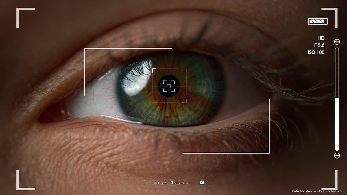
PRIMA retinal implant restores vision in patients with advanced GA

The editorial was authored by Jacque L. Duncan, MD, professor of ophthalmology and chair of the Department of Ophthalmology, University of California, San Francisco, who did not participate in the PRIMA study.

In a press release issued by Science Corporation, the company described the implant as “consisting of a tiny wireless chip implanted in the retina combined with a pair of special glasses, based on work conducted by Professor Daniel Palanker at Stanford University.”

A total of 38 patients were included in the study. All underwent implantation of the PRIMAretinal prosthetic chip with the goal of restoring vision.

Supersized quantum sensors make faint photons easier to catch

Our everyday life is flooded with photons, the quantum building blocks of light. For cutting-edge technology, from quantum computing to deep-tissue imaging, detecting every single photon counts.

“Photons carry information,” said Kristen Parzuchowski, a postdoctoral researcher at the National Institute of Standards and Technology. “Whenever a photon comes into your measurement system, you need to be able to detect it.”

Photons can transmit data in quantum networks or across deep-space communication links. Catching and analyzing photons lets scientists build biomedical images and search the universe for dark matter.

Deuterium enables chip waveguides to generate broadband light from infrared pulses

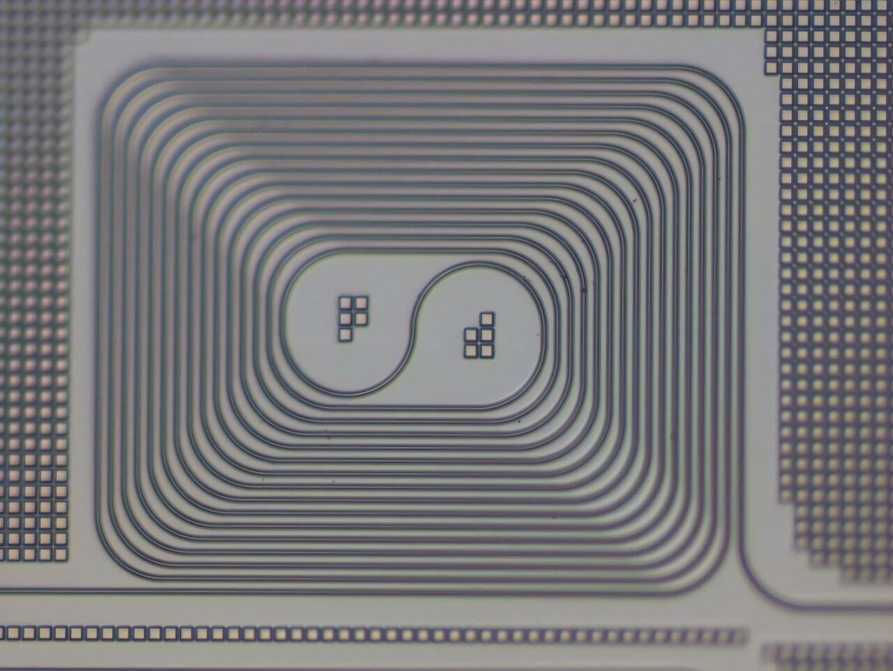
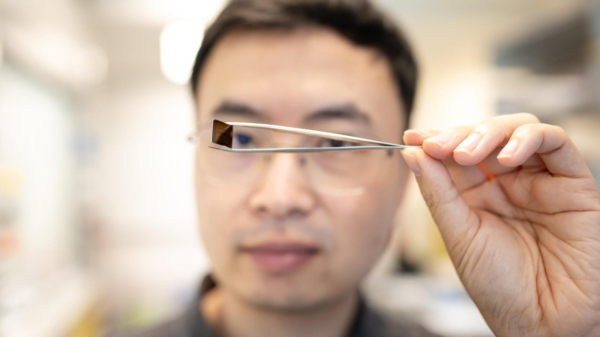
A research team from Singapore, led by Associate Professor Dawn Tan of the Singapore University of Technology and Design (SUTD) and Dr. Luo Xianshu, head of the Silicon Photonics Department at the A*STAR Institute of Microelectronics (A*STAR IME), has developed a low-loss silicon nitride waveguide that generates broadband light on a chip. By replacing hydrogen with its heavier isotope, deuterium, the team fabricated the low-loss SiN waveguide on an 8-inch wafer using a low-temperature process, demonstrating its potential for large-scale manufacturing and integration with CMOS-compatible semiconductor processes.

Published in Optics Express, the paper “Octave-spanning supercontinuum generation in a wafer-scale, low loss deuterated silicon nitride waveguide” demonstrates a chip-scale waveguide that stretches infrared laser pulses into a spectrum running from visible red to deep into the infrared.

Lasers are prized for their color purity because they emit light in a single color, but many of the most demanding technologies require a beam that spans an enormous sweep of the spectrum at once. This so-called supercontinuum light underpins high-resolution medical imaging, precision measurement and the frequency combs that keep optical clocks ticking without error.

This Grain-of-Rice-Sized “Rainbow” Chip Could Transform 6G Communications

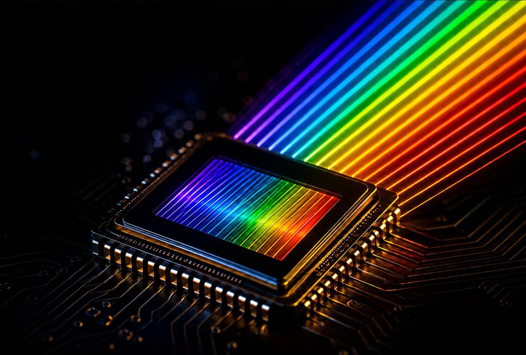
A tiny chip that produces a precisely organized “rainbow” of light could help enable faster, higher-capacity 6G communications and more precise timing for quantum technologies.

A microchip about the size of a grain of rice can generate a carefully ordered spectrum of light and convert it into multiple high-frequency electromagnetic signals called millimeter waves. Physicists at Loughborough University and their international collaborators say the approach could eventually support technologies that require large amounts of bandwidth and exceptionally precise signals.

Millimeter waves are especially attractive for future communications because they provide far more bandwidth, effectively creating additional capacity for transmitting data. The challenge has been producing these frequencies with the precision and stability required for advanced systems.

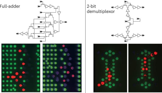
Living circuit boards built by printing bacterial transistors

It points toward a future in which computation isn’t necessarily confined to silicon. Instead, we could build living materials that sense, communicate, compute, and respond—with the “circuit board” itself made of living cells.


Electronic circuit boards carry out different operations on the basis of the configuration of their components. Now, equivalent biological circuits are engineered that compute functions on the basis of the spatial arrangement of different bacterial strains printed on a surface.

/* */