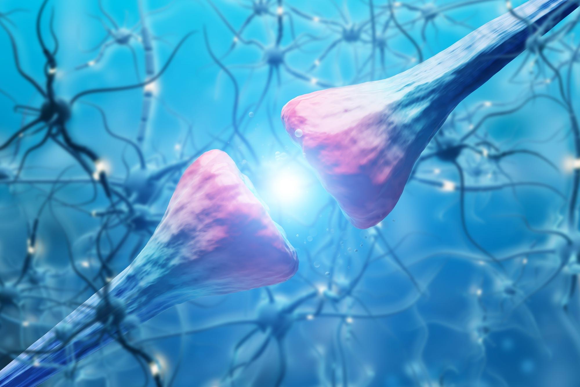
Individual human neurons may be far more powerful computing units than previously understood.
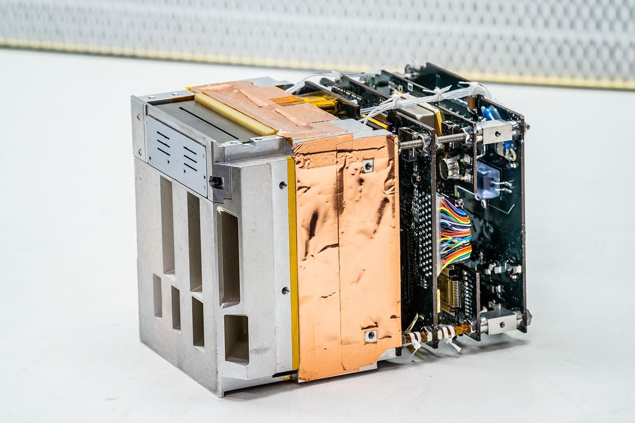
Successfully launched on July 23, 2025, the REAL instrument can distinguish between these potential modes, making it possible to investigate their relative importance and determine which, if any, waves are responsible for electron fallout. Leveraging recent advancements in sensor miniaturization, the instrument includes three sensor heads — a low-, medium-, and high-energy head with two, five, and four simultaneous look directions, respectively — integrated with four electronic boards. Together, they occupy only about half of the REAL CubeSat and use a time resolution sufficient to resolve microbursts of electrons with energies ranging from 40 keV up to 2 MeV. As its parent 3U CubeSat flies in LEO, REAL points along Earth’s magnetic field and can simultaneously measure the quantity, energy, and angle of the particles as they fall into the atmosphere — a first-of-its-kind capability.
“Most CubeSats can observe particles from only a single direction, so they have to spin in order to build up a full picture — and that takes a few seconds, too slow to capture microbursts,” said space physicist Robyn Millan of Dartmouth College, who serves as the REAL mission principal investigator. “With REAL, we’ve managed to squeeze three sensors, each with multiple look directions, into the top of this 100-by-100-millimeter head, allowing us to capture those measurements all at once. We’re really proud of that.”
The high-energy head consists of a 30-millimeter-thick aluminum collimator with four apertures, each spanning 20 degrees of pitch angle. Each aperture connects to an active area on a solid-state detector (SSD) at the base. The medium-energy head similarly uses an SSD base but instead employs five active areas that connect to a 22-millimeter-thick aluminum collimator with five apertures, each spanning 20 degrees of pitch angle. The low-energy head, on the other hand, is a miniature electrostatic analyzer (ESA) consisting of titanium electrodes sandwiched between etched silicon selector slits. These lie on top of a microchannel plate (MCP). The low-energy head uses 36 apertures, two look directions (±40 degrees), and 15 channels to measure electrons with lower energies, from 1 keV to 40 keV.
Quantum computers, devices that process information by leveraging the laws of quantum mechanics, have been found to outperform classical computers in some advanced tasks. Instead of storing information in the form of classical binary bits (i.e., 0 or 1), quantum computers rely on quantum bits (i.e., qubits), which can also exist in combinations of 0 and 1 states.
Despite their potential, quantum computers are known to be highly prone to errors. This is because qubits are very sensitive to heat, magnetic fields and other changes in their surroundings, which can disrupt the delicate quantum states they rely on to store and process data.
Researchers at Princeton University recently introduced a new approach for developing quantum computers that make fewer errors and whose errors are easier to detect and correct.
Quantum computers, systems that process information using the principles of quantum mechanics, could solve some problems that cannot be tackled by the classical computers currently used worldwide. Despite their potential, verifying that these computers are working correctly and can reliably perform computations remains challenging.
Shubhayan Sarkar, a researcher at the University of Gdansk, recently introduced a new scheme for certifying that quantum chips (unitary gates) in a quantum computer are operating correctly without relying on assumptions about their internal components. This scheme, introduced in a paper published in Physical Review Letters, uses an approach referred to as almost device-independent (DI) certification.
“Consider the computer you are using right now,” Sarkar told Phys.org. “If it provides the answer to a mathematical problem, how do you know that the computation is correct? In practice, we rarely verify every calculation ourselves.

For decades, pathologists have diagnosed and graded breast cancer by looking at tissue samples under a microscope, searching for telltale signs of disorder in the structure of cells and tissues. Now, researchers at Columbia and their collaborators have developed a new computational approach that transforms those visual patterns into quantitative measurements, potentially improving how clinicians predict breast cancer outcomes and choose therapies.
In a recent study published in Cancer Research, researchers used mathematical tools known as topology to develop biomarkers quantifying the organizational structure of breast cancer tissue. The approach generated continuous numerical scores that predicted patient survival and treatment response more accurately than many traditional biomarkers, while also showing less variation across racial and ethnic groups.

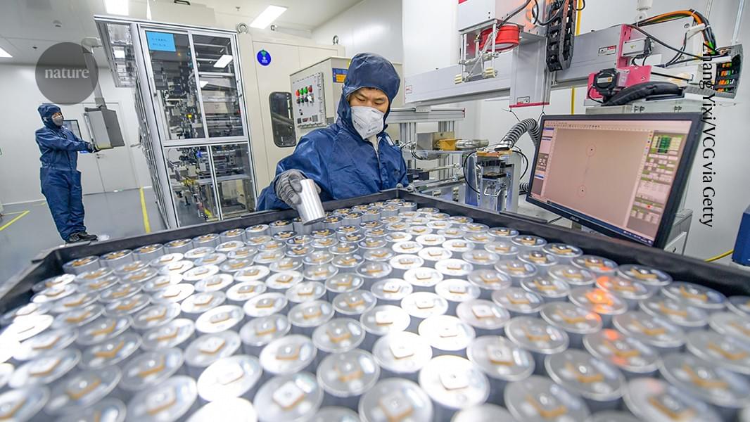
The lithium-ion battery is the beating heart of the modern world. It powers eight billion mobile phones, hundreds of millions of laptops and rapidly growing fleets of electric cars and energy-storage banks. But there’s a new contender breaking into the battery market.
Batteries based on sodium promise to be cheaper, safer and much more environmentally friendly than lithium-ion cells. And this year could mark the start of the sodium era.
In April, Chinese firm CATL — the world’s largest battery producer — announced that it will start mass-producing sodium-ion batteries before the end of 2026. CATL, which is headquartered in Ningde, added that it had signed deals to sell the batteries both to a car manufacturer and to a provider of energy-storage stations for electricity grids.