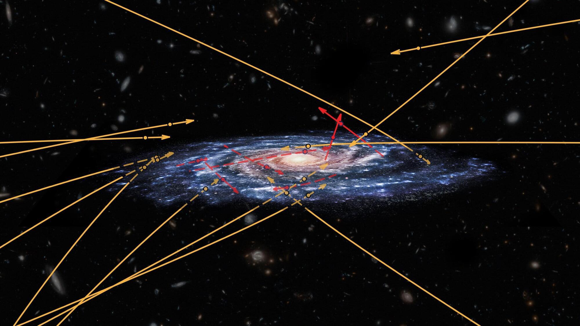
Hypervelocity stars have, since the 1920s, been an important tool that allows astronomers to study the properties of the Milky Way galaxy, such as its gravitational potential and the distribution of matter. Now astronomers from China have made a large-volume search for hypervelocity stars by utilizing a special class of stars known for their distinct, regular, predictable pulsation behavior that makes them useful as distance indicators.
Their research is published in The Astrophysical Journal.
The escape velocity of any planet, star or galaxy is the velocity required for a mass, leaving the object’s surface, to coast completely and exactly out of the planet’s gravitational well, going to infinity. Earth’s escape velocity is 11.2 kilometers per second (km/s).


