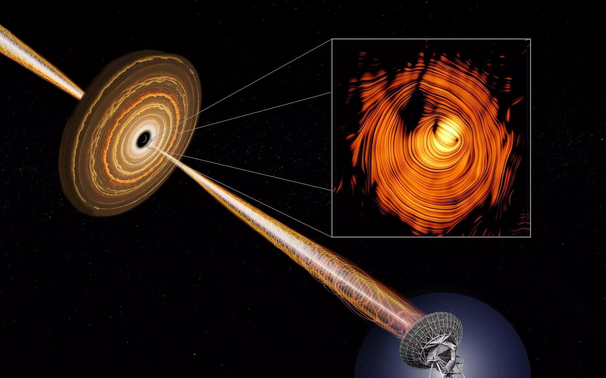
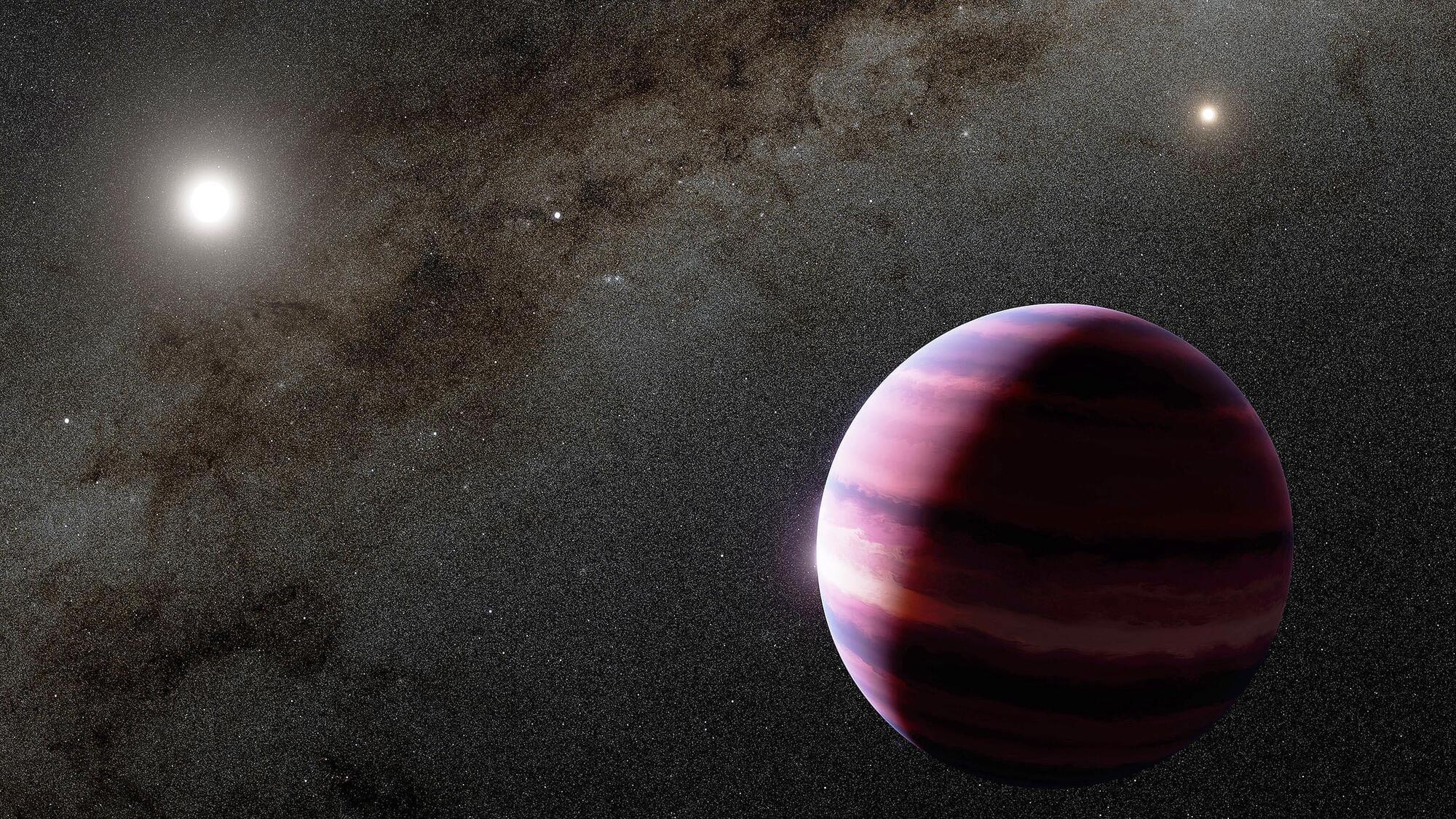
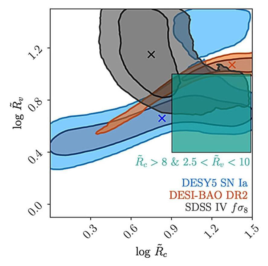
A University of Queensland researcher has developed a new mathematical model to explain the evolution of the universe which, for the first time, includes collapsing regions of matter and expanding voids.

More than 50 years after the last manned moon mission, the Apollo program is still making groundbreaking discoveries.
Lunar rock collected by Apollo 17 is revealing more about the Light Mantle, a distinctive bright streak across the moon’s surface. It’s believed to be the remains of an ancient landslide that happened in the distant past, but the exact cause is unknown.
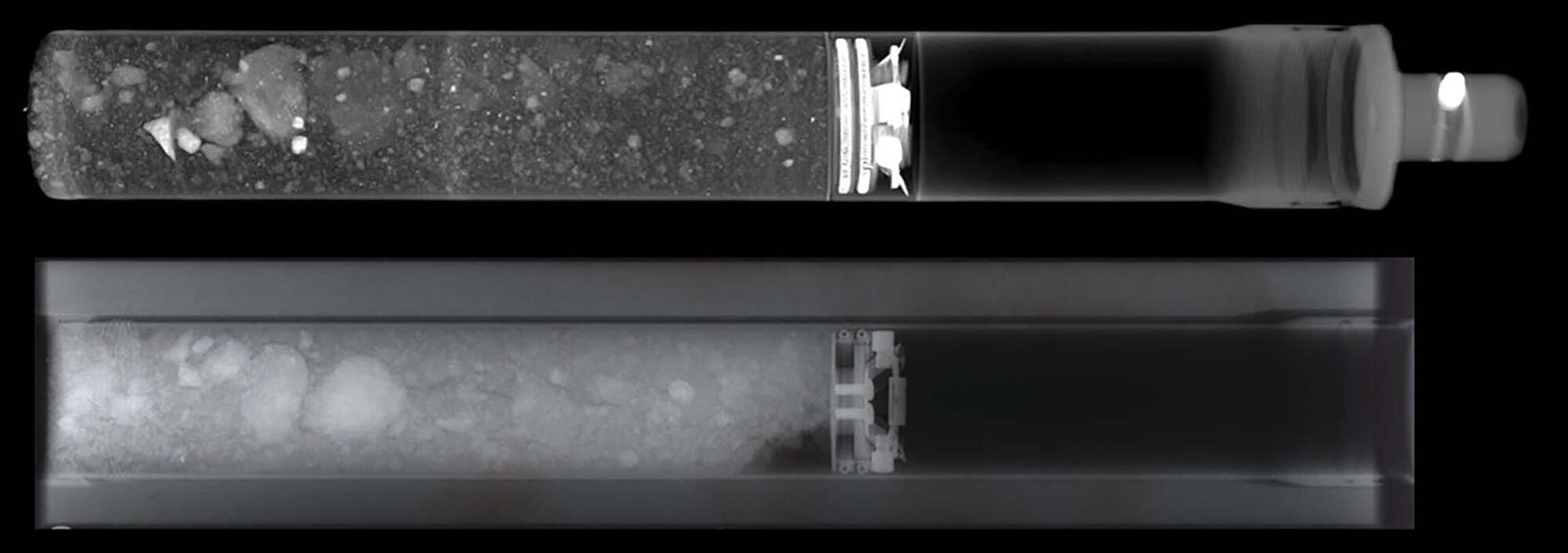
Asteroid strikes, debris from a nearby mountain and seismic activity are all possibilities, but orbital photographs can only reveal so much. Scientists are now studying a rock core from Apollo 17 that was recently unsealed for the first time in 50 years, allowing new insights into the geology of the area.


Scientists unveil nuclear battery with 50-year lifespan and triple efficiency.
Researchers in China have developed a novel nuclear battery that can withstand at least half a century of radiation and deliver three times the energy efficiency of conventional designs.
The team set out to improve battery performance in extreme environments, led by Haisheng San, PhD, a professor at Xiamen University, and Xin Li, PhD, a researcher at the China Institute of Atomic Energy.
According to the scientists, conventional power systems, especially those used in extreme conditions such as space or deep-sea infrastructure, struggle with long-term reliability.


The sky at night. It inspires awe. It inspires thoughts of an existential nature: Who are we? Why are we here? And, perhaps most importantly of all, in which direction should I roll this big ball of shit? That is, if you’re a dung beetle.
“African ball-rolling dung beetles exploit the [Sun], the [Moon], and the celestial polarization pattern to move along straight paths, away from the intense competition at the dung pile,” wrote the study authors. “Even on clear moonless nights, many beetles still manage to orientate along straight paths. This led us to hypothesize that dung beetles exploit the starry sky for orientation, a feat that has, to our knowledge, never been demonstrated in an insect.”
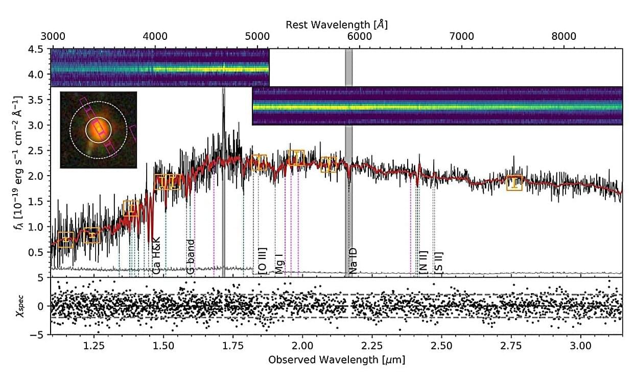
By analyzing the data from the James Webb Space Telescope (JWST) and the Hubble Space Telescope (HST), astronomers from the University of Wisconsin-Madison and elsewhere have probed the properties of a massive and old galaxy designated SMILES-GS-191748. Results of the study, published August 7 on the pre-print server arXiv, shed more light on the nature of this galaxy.
SMILES-GS-191748 is a massive and quiescent galaxy at a redshift of 2.675. The galaxy most likely contains a very old stellar population that first formed when the universe was young.
Given that very little is known about the properties of SMILES-GS-191748, a team of astronomers led by University of Wisconsin-Madison’s Ian McConachie decided to inspect this galaxy using JWST and HST. They nicknamed SMILES-GS-191748 “Eridu,” after the ancient Bronze Age Sumerian city in Mesopotamia due to the galaxy’s suspected early formation time and apparent quiescent nature.
