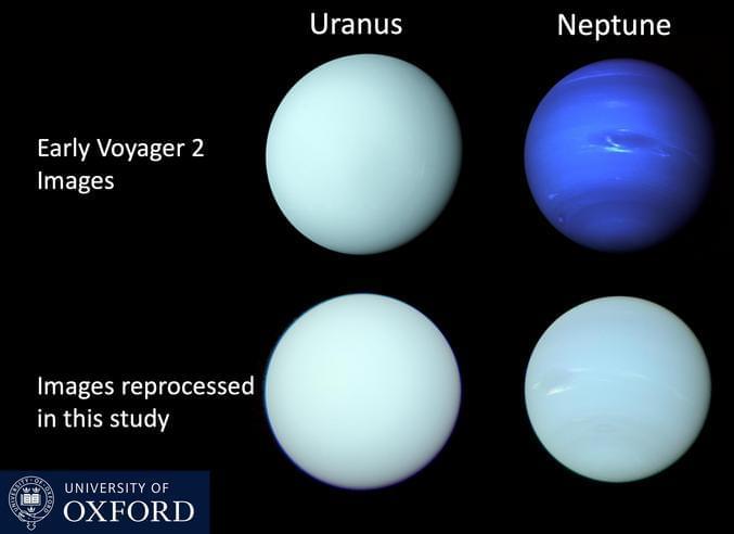
Toggle light / dark theme

Scientists have discovered the brightest energy burst ever detected in space — and Astronomy Twitter is abuzz over the electrifying finding.

As Vice reports, this uber-bright gamma ray burst (GRB), which are huge bursts of energy that occur during major galactic events such as star deaths, was detected by both NASA’s Fermi Gamma-ray Space Telescope and the Neil Gehrels Swift Observatory at England’s University of Leicester.

“Brightest GRB ever just dropped,” University of Alabama astrophysicist Marcos Santander tweeted.

Get a Wonderful Person Tee: https://teespring.com/stores/whatdamath.
More cool designs are on Amazon: https://amzn.to/3wDGy2i.
Alternatively, PayPal donations can be sent here: http://paypal.me/whatdamath.

Hello and welcome! My name is Anton and in this video, we will talk about a discovery of a huge galactic structure behind the Milky Way in the hidden Zone of Avoidance.
Links:
https://arxiv.org/pdf/2210.16332.pdf.
https://en.wikipedia.org/wiki/Zone_of_Avoidance.
Great attractor mystery: https://youtu.be/xAS-IoKLddU
Great debate: https://youtu.be/kcKOV7IwlNc.
#zoneofavoidance #milkyway #mystery.

Support this channel on Patreon to help me make this a full time job:
https://www.patreon.com/whatdamath.

Bitcoin/Ethereum to spare? Donate them here to help this channel grow!

Astronomers have detected an enormous extragalactic structure hiding in an uncharted region of space far beyond the Milky Way ‘s center.

This phantom region, known as the zone of avoidance, is a blank spot on our map of the universe, comprising somewhere between 10% and 20% of the night sky. The reason we can’t see it — at least with standard visible light telescopes — is because the Milky Way’s bulging center blocks our view of it; the center of our galaxy is so dense with stars, dust and other matter that light from the zone of avoidance gets scattered or absorbed before reaching Earth’s telescopes.

However, researchers have had better luck uncovering the zone’s secrets with telescopes that can detect infrared radiation — a type of energy that’s invisible to human eyes, but powerful enough to shine through dense clouds of gas and dust. Infrared surveys of the zone of avoidance have found evidence of thousands of individual galaxies shining through the cosmic fog, though little is known about the large-scale structures that lurk there.

Researchers from LP3 Laboratory in France developed a light-based technique for local material processing anywhere in the three-dimensional space of semiconductor chips. The direct laser writing of new functionalities opens the possibility to exploit the sub-surface space for higher integration densities and extra functions.

Semiconductors remain the backbone material of the electronics integrated with modern devices such as cellphones, cars, robots and many other intelligent devices. Driven by the continuous need for miniaturized and powerful chips, the current semiconductor manufacturing technologies are facing increasing pressure.

The dominating manufacturing technology, lithography, has strong limitations when addressing these challenges, given its surface processing nature. For this reason, a solution to fabricating structures under the wafer surfaces would be highly desirable so that the full space inside the materials could be exploited.

Combinatorial problems often arise in puzzles, origami, and metamaterial design. Such problems have rare collections of solutions that generate intricate and distinct boundaries in configuration space. Using standard statistical and numerical techniques, capturing these boundaries is often quite challenging. Is it possible to flatten a 3D origami piece without causing damage? This question is one such combinatorial issue. As each fold needs to be consistent with flattening, such results are difficult to predict simply by glancing at the design. To answer such questions, the UvA Institute of Physics and the research center AMOLF have shown that researchers may more effectively and precisely respond to such queries by using machine learning techniques.

Despite employing severely undersampled training sets, Convolutional Neural Networks (CNNs) can learn to distinguish these boundaries for metamaterials in minute detail. This raises the possibility of complex material design by indicating that the network infers the underlying combinatorial rules from the sparse training set. The research team thinks this will facilitate the development of sophisticated, functional metamaterials with artificial intelligence. The team’s recent study examined the accuracy of forecasting the characteristics of these combinatorial mechanical metamaterials using artificial intelligence. Their work has also been published in the Physical Review Letters publication.

The attributes of artificial materials, which are engineered materials, are governed by their geometrical structure rather than their chemical makeup. Origami is one such metamaterial. The capacity of an origami piece to flatten is governed by how it is folded, i.e., its structure, and not by the sort of paper it is made of. More generally, the clever design enables us to accurately regulate a metamaterial’s bending, buckling, or bulging. This can be used for many different things, from satellite solar panels that unfurl to shock absorbers.

In an unprecedented experiment, two teams of scientists on either sides of the Atlantic have replicated a material that was previously not produced anywhere on Earth.

As NPR reports, the replication of this powerful compound could have huge implications not just for the manufacturing of high-end machinery, but also for international relations to boot.

Called tetrataenite, the primarily iron-and-nickel compound is normally able to cool for millions of years as it tumbles around in asteroids. As a press release out of the University of Cambridge notes, the researchers who worked in tandem with Boston’s Northeastern University found that if they add phosphorous to the mix, they were able to make synthetic tetrataenite.