Quantum tools in python.
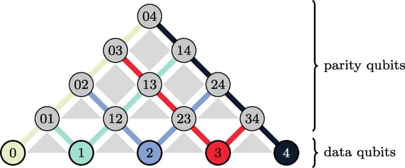
Quantum Toolbox in Python. QuTiP has 12 repositories available. Follow their code on GitHub.
Understanding how matter interacts with light—its optical properties—is critical in a myriad of energy and biomedical technologies, such as targeted drug delivery, quantum dots, fuel combustion, and cracking of biomass. But calculating these properties is computationally intensive, and the inverse problem—designing a structure with desired optical properties—is even harder.
Now Berkeley Lab scientists have developed a machine learning model that can be used for both problems—calculating optical properties of a known structure and, inversely, designing a structure with desired optical properties. Their study was published in Cell Reports Physical Science.
“Our model performs bi-directionally with high accuracy and its interpretation qualitatively recovers physics of how metal and dielectric materials interact with light,” said corresponding author Sean Lubner.
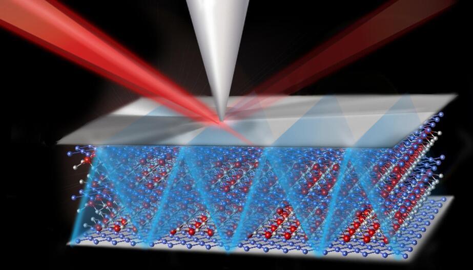
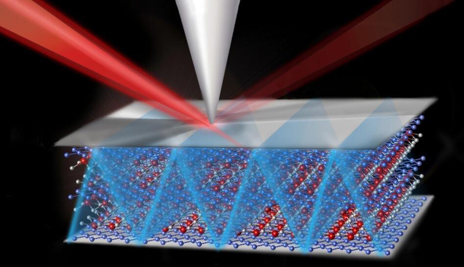
A new tool that uses light to map out the electronic structures of crystals could reveal the capabilities of emerging quantum materials and pave the way for advanced energy technologies and quantum computers, according to researchers at the University of Michigan, University of Regensburg and University of Marburg.
A paper on the work is published in Science.
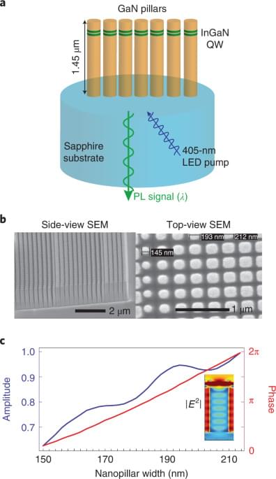
Applications include LED lights, solar cells and artificial photosynthesis.
Graphene, an atomically thin carbon layer through which electrons can travel virtually unimpeded, has been extensively studied since its first successful isolation more than 15 years ago. Among its many unique properties is the ability to support highly confined electromagnetic waves coupled to oscillations of electronic charge—plasmon polaritons—that have potentially broad applications in nanotechnology, including biosensing, quantum information, and solar energy.
However, in order to support plasmon polaritons, graphene must be charged by applying a voltage to a nearby metal gate, which greatly increases the size and complexity of nanoscale devices. Columbia University researchers report that they have achieved plasmonically active graphene with record-high charge density without an external gate. They accomplished this by exploiting novel interlayer charge transfer with a two-dimensional electron-acceptor known as α-RuCl3. The study is available now online as an open access article and will appear in the December 9th issue of Nano Letters.
“This work allows us to use graphene as a plasmonic material without metal gates or voltage sources, making it possible to create stand-alone graphene plasmonic structures for the first time” said co-PI James Hone, Wang Fong-Jen Professor of Mechanical Engineering at Columbia Engineering.
Coherence times in quantum computing have increased by orders of magnitude since the early 2000s. If this exponential progress continues, coherence times measured in seconds or even minutes could be achieved in the near future.
When discussing the latest quantum computers, most people tend to focus on the number of quantum bits (or qubits) in a system. However, while qubit counts are a very important factor, another key metric is coherence time, which measures how long a qubit can hold information.
In order to generate complex mathematical calculations, a qubit needs to hold information for as long as possible. That requires physical qubits to remain highly isolated from the surrounding environment. When a qubit is disrupted by external stimuli – such as background noise from vibrations, temperature changes or stray electromagnetic fields – information about the state of that qubit “leaks out” in a process known as decoherence. This can ruin the ability to exploit any quantum effects. Longer coherence times enable more quantum gates to be utilised before this occurs, resulting in more complex calculations.
Researchers are a step closer to realizing a new kind of memory that works according to the principles of spintronics which is analogous to, but different from, electronics. Their unique gallium arsenide-based ferromagnetic semiconductor can act as memory by quickly switching its magnetic state in the presence of an induced current at low power. Previously, such current-induced magnetization switching was unstable and drew a lot of power, but this new material both suppresses the instability and lowers the power consumption too.
The field of quantum computing often gets covered in the technical press; however, another emerging field along similar lines tends to get overlooked, and that is spintronics. In a nutshell, spintronic devices could replace some electronic devices and offer greater performance at far low power levels. Electronic devices use the motion of electrons for power and communication. Whereas spintronic devices use a transferable property of stationary electrons, their angular momentum, or spin. It’s a bit like having a line of people pass on a message from one to the other rather than have the person at one end run to the other. Spintronics reduces the effort needed to perform computational or memory functions.
Spintronic-based memory devices are likely to become common as they have a useful feature in that they are nonvolatile, meaning that once they are in a certain state, they maintain that state even without power. Conventional computer memory, such as DRAM and SRAM made of ordinary semiconductors, loses its state when it’s powered off. At the core of experimental spintronic memory devices are magnetic materials that can be magnetized in opposite directions to represent the familiar binary states of 1 or 0, and this switching of states can occur very, very quickly. However, there has been a long and arduous search for the best materials for this job, as magnetizing spintronic materials are no simple matter.
Researchers have recently displayed the interaction of superconducting qubits; the basic unit of quantum information, with surface acoustic wave resonators; a surface-wave equivalent of the crystal resonator, in quantum physics. This phenomena opens a new field of research, defined as quantum acoustodynamics to allow the development of new types of quantum devices. The main challenge in this venture is to manufacture acoustic resonators in the gigahertz range. In a new report now published on Nature Communications Physics, Aleksey N. Bolgar and a team of physicists in Artificial Quantum Systems and Physics, in Russia and the U.K., detailed the structure of a significantly simplified hybrid acoustodynamic device by replacing an acoustic resonator with a phononic crystal or acoustic metamaterial.
The crystal contained narrow metallic stripes on a quartz surface and this artificial atom or metal object in turn interacted with a microwave transmission line. In engineering, a transmission line is a connector that transmits energy from one point to another. The scientists used the setup to couple two degrees of freedom of different nature, i.e. acoustic and electromagnetic, with a single quantum object. Using a scattering spectrum of propagating electromagnetic waves on the artificial atom they visualized acoustic modes of the phononic crystal. The geometry of the device allowed them to realize the effects of quantum acoustics on a simple and compact system.