Support the Research Behind this Channel on Patreon:
/ arvinash.
REFERENCES
How black holes may be responsible for Dark Energy • How BLACK HOLES May be Responsible for DAR…
Is Dark Energy made of particles? • Is Dark ENERGY made of PARTICLES? The Quin…
What is Dark Energy made of? • What is Dark Energy made of? Quintessence?… CHAPTERS 0:00 The 70% mystery 0:58 How Dark Energy was discovered? 4:26 What could be causing Dark Energy? 6:58 Repulsive Gravity? 10:16 What is the energy made of? 11:56 Evolving Dark energy? Quintesssence 14:18 Could Dark Energy be a particle? 16:43 Could Black Holes cause Dark Energy? SUMMARY Dark energy is one of the greatest mysteries in modern physics. It appears to make up nearly 70% of the universe, yet scientists still do not know what it is. Unlike matter, it does not clump together. Unlike radiation, it does not dilute as space expands. Instead, it causes the expansion of the universe to accelerate, pushing galaxies apart faster over time. The discovery of this acceleration came in the late 1990s when astronomers measured distant Type Ia supernovae, which act as reliable “standard candles.” By comparing their brightness and redshift, researchers could determine how fast the universe expanded at different points in cosmic history. Instead of finding that gravity slowed expansion—as expected—they discovered the opposite: the universe was expanding faster and faster. This unexpected result led to the concept of dark energy, the unknown driver behind cosmic acceleration. One possible explanation is that dark energy is a cosmological constant, represented by the Greek letter lambda in Einstein’s equations. In this model, empty space itself contains a constant energy density known as vacuum energy. Quantum mechanics predicts that empty space is not truly empty; quantum fields constantly fluctuate, producing short-lived “virtual particles.” These fluctuations create energy even in a vacuum. Experiments like the Casimir effect provide evidence that vacuum energy is real. However, this explanation has a major problem. When physicists calculate vacuum energy using quantum theory, the predicted value is about 10¹²⁰ times larger than what observations of the universe allow. This enormous mismatch is widely considered the worst prediction in physics. In general relativity, cosmic acceleration can occur if the universe contains energy with negative pressure. In the Friedmann equation, expansion accelerates when pressure is sufficiently negative relative to energy density. Dark energy appears to have exactly this property, effectively producing a form of repulsive gravity that stretches spacetime. Another possibility is that dark energy is not constant but comes from a dynamic field known as quintessence. In quantum theory, fields can have particle-like excitations, meaning dark energy might correspond to extremely weakly interacting particles. If the strength of this field changes over time, the acceleration of the universe could grow stronger. In extreme scenarios, this could eventually lead to a catastrophic future known as the Big Rip, where galaxies, stars, atoms, and even spacetime itself are torn apart. A more speculative idea suggests a connection between supermassive black holes and dark energy. Some recent studies have observed that black holes appear to grow more massive over billions of years than expected from normal matter accretion alone. Researchers have proposed that black holes might somehow be linked to dark energy, though current evidence only shows a correlation and not a confirmed causal explanation. #darkenergy For now, dark energy remains an observed phenomenon with multiple possible explanations. Whether it is a property of empty space, a new field of physics, or something even deeper, it stands as one of the most profound open questions in cosmology.
CHAPTERS
0:00 The 70% mystery
0:58 How Dark Energy was discovered?
4:26 What could be causing Dark Energy?
6:58 Repulsive Gravity?
10:16 What is the energy made of?
11:56 Evolving Dark energy? Quintesssence
14:18 Could Dark Energy be a particle?
16:43 Could Black Holes cause Dark Energy?
SUMMARY
Dark energy is one of the greatest mysteries in modern physics. It appears to make up nearly 70% of the universe, yet scientists still do not know what it is. Unlike matter, it does not clump together. Unlike radiation, it does not dilute as space expands. Instead, it causes the expansion of the universe to accelerate, pushing galaxies apart faster over time.
The discovery of this acceleration came in the late 1990s when astronomers measured distant Type Ia supernovae, which act as reliable “standard candles.” By comparing their brightness and redshift, researchers could determine how fast the universe expanded at different points in cosmic history. Instead of finding that gravity slowed expansion—as expected—they discovered the opposite: the universe was expanding faster and faster. This unexpected result led to the concept of dark energy, the unknown driver behind cosmic acceleration.
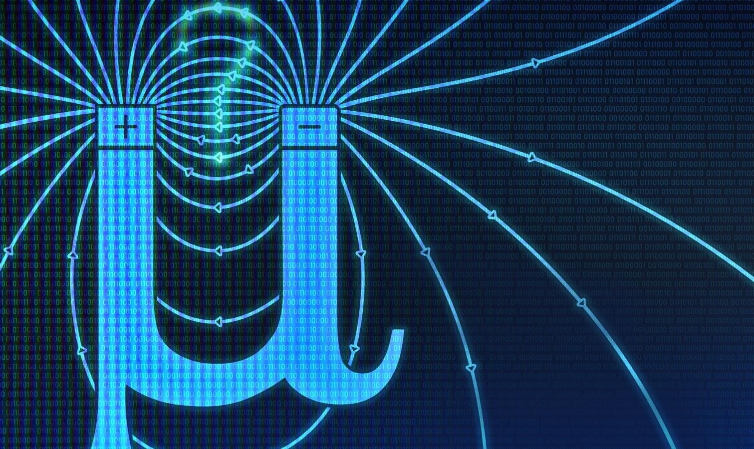
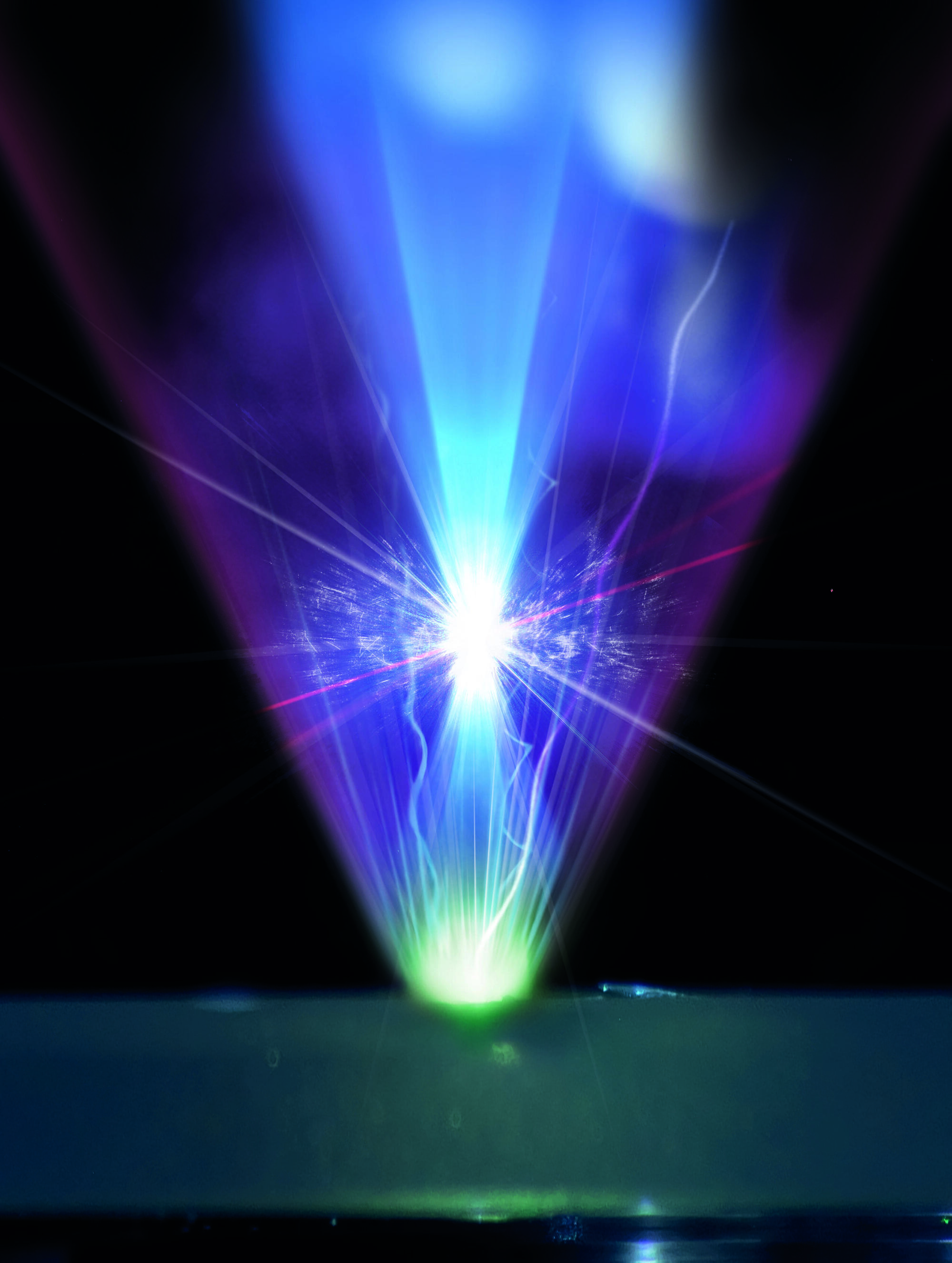
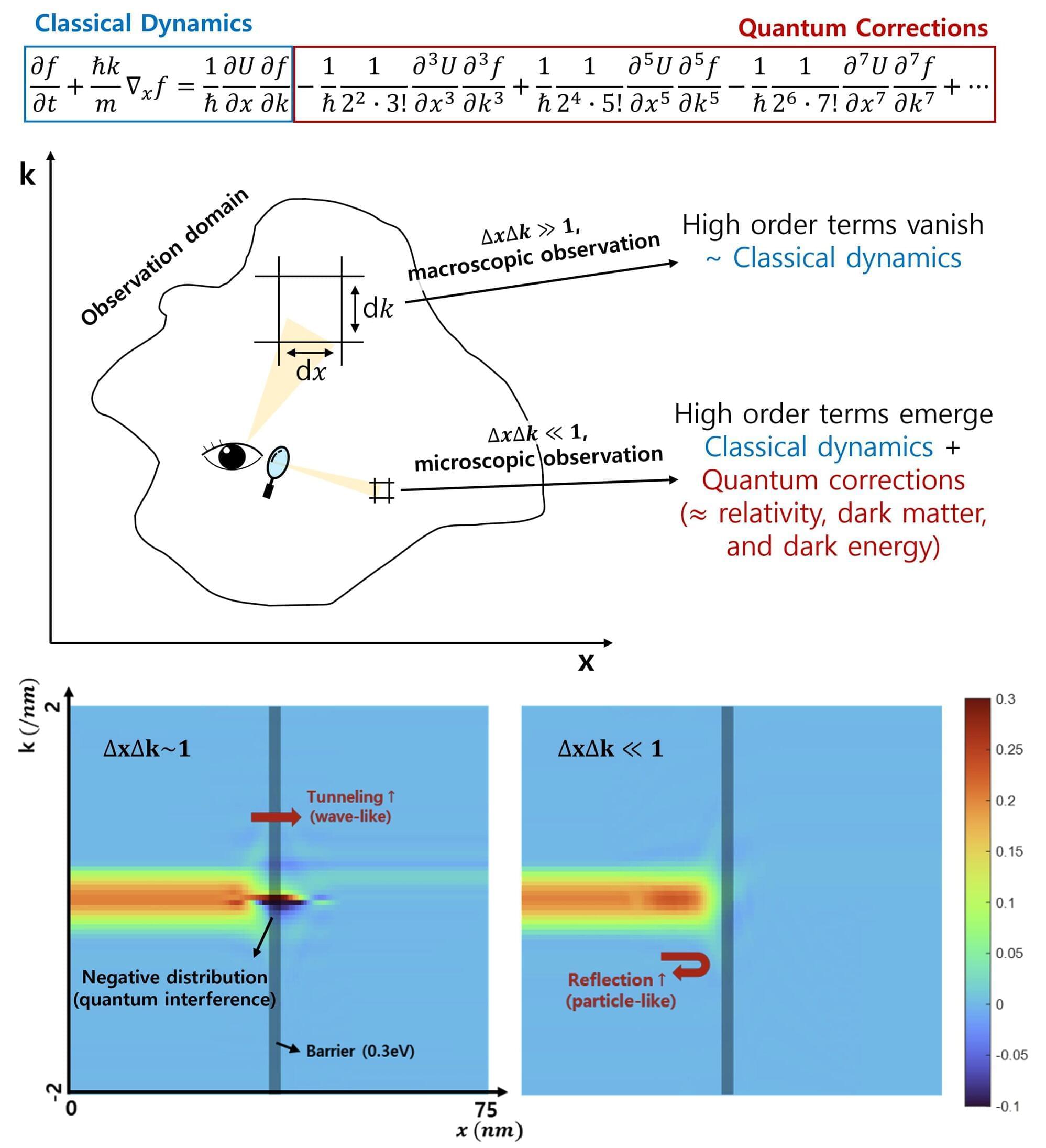
One possible explanation is that dark energy is a cosmological constant, represented by the Greek letter lambda in Einstein’s equations. In this model, empty space itself contains a constant energy density known as vacuum energy. Quantum mechanics predicts that empty space is not truly empty; quantum fields constantly fluctuate, producing short-lived “virtual particles.” These fluctuations create energy even in a vacuum. Experiments like the Casimir effect provide evidence that vacuum energy is real.