Toggle light / dark theme

Freestanding hafnium zirconium oxide membranes can enable advanced 2D transistors

To further reduce the size of electronic devices, while also improving their performance and energy efficiency, electronics engineers have been trying to identify alternative materials that outperform silicon and other conventional semiconductors. Two-dimensional (2D) semiconductors, materials that are just a few atoms thick and have a tunable electrical conductivity, are among the most promising candidates for the fabrication of smaller and better performing devices.

Past studies showed that these materials could be used to fabricate miniaturized transistors, electronic components that amplify or switch , particularly field-effect transistors (FETs). These are transistors that control the flow of electrical current using an electric field.

To reliably operate, however, FETs also need to integrate an insulating layer that separates the so-called gate electrode (i.e., the terminal regulating the flow of current) from the channel (i.e., the pathway through which electrical current flows). To enable greater control over the gate, this insulating layer, known as a , should have a high dielectric constant (κ), or in other words, it should effectively store electrical energy.

Particle pattern reveals how desert dust facilitates ice formation in clouds

A new study shows that natural dust particles swirling in from faraway deserts can trigger freezing of clouds in Earth’s Northern Hemisphere. This subtle mechanism influences how much sunlight clouds reflect and how they produce rain and snow—with major implications for climate projections.

Measuring three-nucleon interactions to better understand nuclear data and neutron stars

Though atomic nuclei are often depicted as static clusters of protons and neutrons (nucleons), the particles are actually bustling with movement. Thus, the nucleons carry a range of momenta. Sometimes, these nucleons may even briefly engage through the strong interaction. This interaction between two nucleons can boost the momentum of both and form high-momentum nucleon pairs. This effect yields two-nucleon short-range correlations.

Experiments at the U.S. Department of Energy’s Thomas Jefferson National Accelerator Facility have studied these pairs to learn how protons and neutrons preferentially pair up at short distances. However, short-range correlations involving three or more nucleons haven’t been detected yet.

Now, in a study published in Physics Letters B, researchers used data from a 2018 experiment in Jefferson Lab’s Hall A to measure the signature of three– short-range correlations for the first time.

Epochs of the Universe — The Cosmic Clock & Civilization

Explore the entire life story of the cosmos, from quantum flickers at the Big Bang to the distant eras of black holes and dark energy, and discover what kinds of civilizations might endure across these unimaginable spans of time.

Watch my exclusive video Mass Drivers on the Moon: https://nebula.tv/videos/isaacarthur-mass-drivers-on-the-moo…ar-economy.
Get Nebula using my link for 40% off an annual subscription: https://go.nebula.tv/isaacarthur.
Get a Lifetime Membership to Nebula for only $300: https://go.nebula.tv/lifetime?ref=isaacarthur.
Use the link https://gift.nebula.tv/isaacarthur to give a year of Nebula to a friend for just $36.

Visit our Website: http://www.isaacarthur.net.
Join Nebula: https://go.nebula.tv/isaacarthur.
Support us on Patreon: https://www.patreon.com/IsaacArthur.
Support us on Subscribestar: https://www.subscribestar.com/isaac-arthur.
Facebook Group: https://www.facebook.com/groups/1583992725237264/
Reddit: https://www.reddit.com/r/IsaacArthur/
Twitter: https://twitter.com/Isaac_A_Arthur on Twitter and RT our future content.
SFIA Discord Server: https://discord.gg/53GAShE
Credits:
Spaceport Innovations — Designing the Next Generation of Launch Sites.
July 31, 2025; Episode 744
Written, Produced & Narrated by: Isaac Arthur.
Epochs of the Universe — The Cosmic Clock & Civilization (July 31, 2025)
Recorded: June 2025
Written by: Isaac Arthur.
Editor: Lukas Konecny.
Select imagery/video supplied by Getty Images.
Music Courtesy of Epidemic Sound http://epidemicsound.com/creator.

Chapters.
0:00 Intro.
2:26 The T-Scale — Time, Terrifyingly Large and Small.
8:25 The Grand Unification Epoch.
10:30 The Inflationary Epoch.
15:40 The Electroweak Epoch.
17:41 The Quark Epoch.
18:19 The Hadron Epoch.
19:28 The Early Universe.
22:52 The Stelliferous Era (T10–T14)
22:24 Into the Darkness (T15-T67)
31:56 The Sojourn.
32:54 The Black Hole Era.
36:55 The Dark Era.
40:29 Final Fates: Cycles, Cracks, and Cosmic Cliffhangers.

New strategy can directly pattern 2D materials into high-quality wafer-scale arrays

Two-dimensional (2D) semiconductors, materials that can conduct electricity and are only a few atoms thick, are promising alternatives to the conventional silicon-based semiconductors currently used to fabricate many electronics. Despite their promise, these materials have not yet been deployed on a large scale.

One reason for this is that reliably synthesizing them and patterning them to produce wafers (i.e., circular substrates employed in the manufacturing of electronics) has so far proved challenging. In fact, many existing patterning techniques rely on or polymer masks, both of which can leave unwanted residues on a wafer or damage the surface of 2D .

Researchers at Nanyang Technological University recently developed a new strategy to pattern 2D films into high-quality wafer-scale arrays, without damaging them or introducing undesirable residues. Their proposed method, outlined in a paper published in Nature Electronics, entails the use of a metal stamp producing three-dimensional (3D) patterns, which can be pressed onto 2D materials to produce a wafer with desired patterns.

Nanotechnology in AI: Building Faster, Smaller, and Smarter Systems

As artificial intelligence (AI) rapidly advances, the physical limitations of conventional semiconductor hardware have become increasingly apparent. AI models today demand vast computational resources, high-speed processing, and extreme energy efficiency—requirements that traditional silicon-based systems struggle to meet. However, nanotechnology is stepping in to reshape the future of AI by offering solutions that are faster, smaller, and smarter at the atomic scale.

The recent article published by AZoNano provides a compelling overview of how nanotechnology is revolutionizing the design and operation of AI systems, pushing beyond the constraints of Moore’s Law and Dennard scaling. Through breakthroughs in neuromorphic computing, advanced memory devices, spintronics, and thermal management, nanomaterials are enabling the next generation of intelligent systems.

Study outlines alternative approach to detecting inelastic dark matter particles

It is now understood that all known matter, i.e., studied by science and harnessed by technology, constitutes only 5% of the content of the universe. The rest is composed of two unknown components: dark matter (about 27%) and dark energy (about 68%). This calculation, confirmed decades ago, continues to surprise both lay people and scientists alike.

In the case of dark matter (DM), there is abundant evidence that it really exists, all resulting from its with ordinary matter. This evidence comes from sources such as the rotation curves of stars in galaxies, discrepancies in the movement of galaxies in clusters, the formation of large-scale structures in the universe, and cosmic background radiation, which is distributed uniformly throughout space.

Despite knowing with a high degree of certainty that DM exists, we do not know what it is. Several models proposed thus far have failed.

Simulations prove early Earth’s liquid core generated protective magnetic field

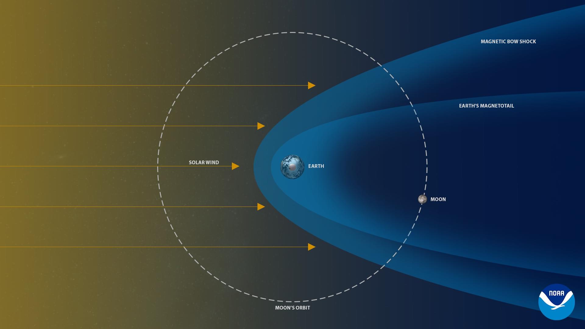
Earth is fortunate in having a magnetic field: it protects the planet and its life from harmful cosmic radiation. Other planets in our solar system—such as Mars—are constantly bombarded by charged particles that make life difficult.

Compact setup successfully detects elusive antineutrinos from nuclear reactor

Neutrinos are extremely elusive elementary particles. Day and night, 60 billion of them stream from the sun through every square centimeter of Earth every second, which is transparent to them. After the first theoretical prediction of their existence, decades passed before they were actually detected. These experiments are usually extremely large to account for the very weak interaction of neutrinos with matter.

Scientists at the Max Planck Institute for Nuclear Physics (MPIK) in Heidelberg have now succeeded in detecting antineutrinos from the reactor of a using the CONUS+ experiment, with a detector mass of just 3 kg. The work is published in Nature.

Originally based at the Brokdorf nuclear power plant, the CONUS experiment was relocated to the Leibstadt nuclear power plant (KKL) in Switzerland in the summer of 2023. Improvements to the 1 kg germanium semiconductor detectors, as well as the excellent measurement conditions at KKL, made it possible for the first time to measure what is known as Coherent Elastic Neutrino-Nucleus Scattering (CEvNS).

Building electronics that don’t die: Columbia’s breakthrough at CERN

Deep beneath the Swiss-French border, the Large Hadron Collider unleashes staggering amounts of energy and radiation—enough to fry most electronics. Enter a team of Columbia engineers, who built ultra-rugged, radiation-resistant chips that now play a pivotal role in capturing data from subatomic particle collisions. These custom-designed ADCs not only survive the hostile environment inside CERN but also help filter and digitize the most critical collision events, enabling physicists to study elusive phenomena like the Higgs boson.

/* */