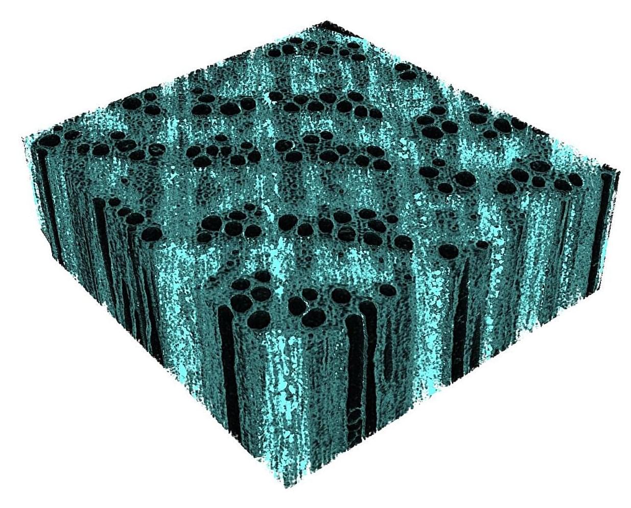
Toggle light / dark theme

Synthetic Biology: George Church on Genome Sequencing and De-Extinction

The great George Church takes us through the revolutionary journey of DNA sequencing from his early groundbreaking work to the latest advancements. He discusses the evolution of sequencing methods, including molecular multiplexing, and their implications for understanding and combating aging.

We talk about the rise of biotech startups, potential future directions in genome sequencing, the role of precise gene therapies, the ongoing integration of nanotechnology and biology, the potential of biological engineering in accelerating evolution, transhumanism, the Human Genome Project, and the importance of intellectual property in biotechnology.

The episode concludes with reflections on future technologies, the importance of academia in fostering innovation, and the need for scalable developments in biotech.

00:00 Introduction to Longevity and DNA Sequencing.
01:43 George Church’s Early Work in Genomic Sequencing.
02:38 Innovations in DNA Sequencing.
03:15 The Evolution of Sequencing Methods.
07:41 Longevity and Aging Reversal.
12:12 Biotech Startups and Commercial Endeavors.
17:38 Future Directions in Genome Sequencing.
28:10 Humanity’s Role and Transhumanism.
37:23 Exploring the Connectome and Neural Networks.
38:29 The Mystery of Life: From Atoms to Living Systems.
39:35 Accelerating Evolution and Biological Engineering.
41:37 Merging Nanotechnology and Biology.
45:00 The Future of Biotech and Young Innovators.
47:16 The Human Genome Project: Successes and Shortcomings.
01:01:10 Intellectual Property in Biotechnology.
01:06:30 Future Technologies and Final Thoughts.

Anti-laser Engineered for Coherent Perfect Absorption of Light

In 2019, researchers from the Massachusetts Institute of Technology made headlines when they created the “blackest black” material made from carbon nanotubes —ten times blacker than any material that had been manufactured at that time—a material so black that it had the ability to absorb 99.995% of incident light. Such research in light absorption is not a trivial pursuit or mere aesthetics, there are many technologies that can benefit from maximizing light absorption—for instance, in photovoltaics because of the need to absorb and convert as much light as possible into electricity, or on the interior surface of a light sensor because of the need to minimize unwanted stray light. The physics of light absorption can get quite complex when you get into the details, as what we non-technically consider as “black” is usually not a perfect absorber. Indeed, there are many ways to create something that can absorb some light, but the endeavor gets increasingly more difficult the closer one attempts to achieve 100% absorption.

That takes some serious physics.

Now, physicists in Austria and Israel report in the journal Science that they have engineered a light trap that utilizes the quantum properties of electromagnetic waves— in which waveforms undergo constructive or destructive interference when combined in just the right manner—to generate an anti-laser that has near-perfect light absorption [1]. Because the light trap functions essentially as a time-reversed laser, where instead of multiple passes of single-wavelength light for maximum stimulated emission of photons the multiple passes are engineered for maximum absorption, the device is a veritable anti-laser.

New technique enhances absorptivity of powders for metal 3D printing

A team from Lawrence Livermore National Laboratory, Stanford University and the University of Pennsylvania introduced a novel wet chemical etching process that modifies the surface of conventional metal powders used in 3D printing.


In a significant advancement for metal additive manufacturing, researchers at Lawrence Livermore National Laboratory (LLNL) and their academic partners have developed a groundbreaking technique that enhances the optical absorptivity of metal powders used in 3D printing.

The innovative approach, which involves creating nanoscale surface features on metal powders, promises to improve the efficiency and quality of printed metal parts, particularly for challenging materials like copper and tungsten, according to researchers.

Additive manufacturing (AM) — more commonly known as 3D printing — has transformed the way products are designed and produced, allowing for the creation of complex geometries and customized components that traditional manufacturing methods struggle to achieve. However, one of the persistent challenges in laser powder-bed fusion (LPBF) metal 3D printing is the high reflectivity of certain metals, which can lead to inefficient energy absorption during the printing process and can even damage some printing machines. This inefficiency often results in inadequate print quality and increased energy consumption, according to researchers.

Assessing polylactic acid nanofibers with cellulose and chitosan nanocapsules loaded with chamomile extract for treating gram-negative infections

This study presents the development and characterization of a novel nanocomposite wound dressing material based on polylactic acid (PLA) nanofibers incorporating chitosan nanocapsules loaded with chamomile extract and cellulose nanoparticles.


Asadzadeh, F., Ghorbanzadeh, S., Poursattar Marjani, A. et al. Sci Rep 14, 22,336 (2024). https://doi.org/10.1038/s41598-024-72398-9

Download citation.

New Nanotechnology AIDS in Electron Cooling Without External Sources

Using a nanoscale structure that consisted of a sequential array of a source electrode, a quantum well, a tunneling barrier, a quantum dot, another tunneling barrier, and a drain electrode, researchers were able to suppress electron excitation and cool electrons to −228 °C (−378 °F) without external means at room temperature.

A team of researchers has discovered a way to cool electrons to −228 °C without external means and at room temperature, an advancement that could enable electronic devices to function with very little energy.

The process involves passing electrons through a quantum well to cool them and keep them from heating.

Brookhaven National Laboratory Scientists Explore Ways to Synchronize Magnetic Spins for Nanoscale Electronic Devices

Brookhaven National Laboratory researchers are working to develop ways to synchronize the magnetic spins in nanoscale devices to build tiny signal-generating or receiving antennas and other electronics.

Upton, New York — Scientists at the U.S. Department of Energy’s Brookhaven National Laboratory are seeking ways to synchronize the magnetic spins in nanoscale devices to build tiny yet more powerful signal-generating or receiving antennas and other electronics. Their latest work, published in Nature Communications, shows that stacked nanoscale magnetic vortices separated by an extremely thin layer of copper can be driven to operate in unison, potentially producing a powerful signal that could be put to work in a new generation of cell phones, computers, and other applications.

The aim of this “spintronic” technology revolution is to harness the power of an electron’s “spin,” the property responsible for magnetism, rather than its negative charge.

Nanotechnology Dramatically Improves Electronic Device Performance

A new study from researchers at Tyndall National Institute and the National University of Singapore shows that subtle changes in the intermolecular van der Waals interactions in the active component of a molecular diode can improve the device performance by more than a factor of ten.

A team of scientists from Tyndall National Institute at University College Cork and the National University of Singapore have designed and fabricated ultra-small devices for energy-efficient electronics. By finding out how molecules behave in these devices, a ten-fold increase in switching efficiency was obtained by changing just one carbon atom. These devices could provide new ways to combat overheating in mobile phones and laptops, and could also aid in electrical stimulation of tissue repair for wound healing. The breakthrough creation of molecular devices with highly controllable electrical properties will appear in the February issue of Nature Nanotechnology. Dr. Damien Thompson at the Tyndall National Institute, UCC and a team of researchers at the National University of Singapore led by Prof. Chris Nijhuis designed and created the devices, which are based on molecules acting as electrical valves, or diode rectifiers.

Dr. Thompson explains “These molecules are very useful because they allow current to flow through them when switched ON and block current flow when switched OFF. The results of the study show that simply adding one extra carbon is sufficient to improve the device performance by more than a factor of ten. We are following up lots of new ideas based on these results, and we hope ultimately to create a range of new components for electronic devices.” Dr. Thompson’s atom-level computer simulations showed how molecules with an odd number of carbon atoms stand straighter than molecules with an even number of carbon atoms. This allows them to pack together more closely. Tightly-packed assemblies of these molecules were formed on metal electrode surfaces by the Nijhuis group in Singapore and were found to be remarkably free of defects. These high quality devices can suppress leakage currents and so operate efficiently and reliably.

/* */