In Switzerland researchers are trying to help tackle the food waste challenge using nanotechnology.


— 300 interviews with the people who shape our world, in 40 countries and on 12 platforms.
Recognise yourself? If so, please RT!
#movethehumanstoryforward #science #arts #culture #music #technology #artificialintelligence #nanotech #quantumphysics #space #blockchain #ideaXme
Circa 2018
Researchers inject tiny devices into the bloodstream to deliver drugs with precision.
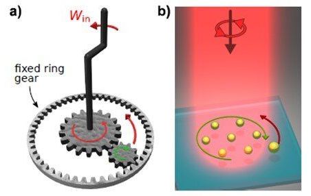
“In previous work, the researchers discovered that when optical matter is exposed to circularly polarized light, it rotates as a rigid body in the direction opposite the polarization rotation. In other words, when the incident light rotates one way the optical matter array responds by spinning the other. This is a manifestation of “negative torque”. The researchers speculated that a machine could be developed based on this new phenomenon.
In the new work, the researchers created an optical matter machine that operates much like a mechanical machine based on interlocking gears. In such machines, when one gear is turned, a smaller interlocking gear will spin in the opposite direction. The optical matter machine uses circularly polarized light from a laser to create a nanoparticle array that acts like the larger gear by spinning in the optical field. This “optical matter gear” converts the circularly polarized light into orbital, or angular, momentum that influences a nearby probe particle to orbit the nanoparticle array (the gear) in the opposite direction.”
Researchers have developed a tiny new machine that converts laser light into work. These optically powered machines self-assemble and could be used for nanoscale manipulation of tiny cargo for applications such as nanofluidics and particle sorting.
“Our work addresses a long-standing goal in the nanoscience community to create self-assembling nanoscale machines that can perform work in conventional environments such as room temperature liquids,” said research team leader Norbert F. Scherer from the University of Chicago.
Scherer and colleagues describe the new nanomachines in Optica. The machines are based on a type of matter known as optical matter in which metal nanoparticles are held together by light rather than the chemical bonds that hold together the atoms that make up typical matter.

Based on optical matter, new machines could be used to move and manipulate tiny particles.
Researchers have developed a tiny new machine that converts laser light into work. These optically powered machines self-assemble and could be used for nanoscale manipulation of tiny cargo for applications such as nanofluidics and particle sorting.
“Our work addresses a long-standing goal in the nanoscience community to create self-assembling nanoscale machines that can perform work in conventional environments such as room temperature liquids,” said research team leader Norbert F. Scherer from the University of Chicago.

One of the most remarkable recent advances in biomedical research has been the development of highly targeted gene-editing methods such as CRISPR that can add, remove, or change a gene within a cell with great precision. The method is already being tested or used for the treatment of patients with sickle cell anemia and cancers such as multiple myeloma and liposarcoma, and today, its creators Emmanuelle Charpentier and Jennifer Doudna received the Nobel Prize in chemistry.
While gene editing is remarkably precise in finding and altering genes, there is still no way to target treatment to specific locations in the body. The treatments tested so far involve removing blood stem cells or immune system T cells from the body to modify them, and then infusing them back into a patient to repopulate the bloodstream or reconstitute an immune response—an expensive and time-consuming process.
Building on the accomplishments of Charpentier and Doudna, Tufts researchers have for the first time devised a way to directly deliver gene-editing packages efficiently across the blood brain barrier and into specific regions of the brain, into immune system cells, or to specific tissues and organs in mouse models. These applications could open up an entirely new line of strategy in the treatment of neurological conditions, as well as cancer, infectious disease, and autoimmune diseases.
Diamonds have a firm foothold in our lexicon. Their many properties often serve as superlatives for quality, clarity and hardiness. Aside from the popularity of this rare material in ornamental and decorative use, these precious stones are also highly valued in industry where they are used to cut and polish other hard materials and build radiation detectors.
More than a decade ago, a new property was uncovered in diamonds when high concentrations of boron are introduced to it: superconductivity. Superconductivity occurs when two electrons with opposite spin form a pair (called a Cooper pair), resulting in the electrical resistance of the material being zero. This means a large supercurrent can flow in the material, bringing with it the potential for advanced technological applications. Yet, little work has been done since to investigate and characterize the nature of a diamond’s superconductivity and therefore its potential applications.
New research led by Professor Somnath Bhattacharyya in the Nano-Scale Transport Physics Laboratory (NSTPL) in the School of Physics at the University of the Witwatersrand in Johannesburg, South Africa, details the phenomenon of what is called “triplet superconductivity” in diamond. Triplet superconductivity occurs when electrons move in a composite spin state rather than as a single pair. This is an extremely rare, yet efficient form of superconductivity that until now has only been known to occur in one or two other materials, and only theoretically in diamonds.
French company Nawa technologies says it’s already in production on a new electrode design that can radically boost the performance of existing and future battery chemistries, delivering up to 3x the energy density, 10x the power, vastly faster charging and battery lifespans up to five times as long.
Nawa is already known for its work in the ultracapacitor market, and the company has announced that the same high-tech electrodes it uses on those ultracapacitors can be adapted for current-gen lithium-ion batteries, among others, to realize some tremendous, game-changing benefits.
It all comes down to how the active material is held in the electrode, and the route the ions in that material have to take to deliver their charge. Today’s typical activated carbon electrode is made with a mix of powders, additives and binders. Where carbon nanotubes are used, they’re typically stuck on in a jumbled, “tangled spaghetti” fashion. This gives the charge-carrying ions a random, chaotic and frequently blocked path to traverse on their way to the current collector under load.
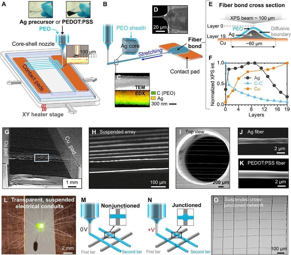
Scalability and device integration have been prevailing issues limiting our ability in harnessing the potential of small-diameter conducting fibers. We report inflight fiber printing (iFP), a one-step process that integrates conducting fiber production and fiber-to-circuit connection. Inorganic (silver) or organic {PEDOT: PSS [poly(3,4-ethylenedioxythiophene) polystyrene sulfonate]} fibers with 1- to 3-μm diameters are fabricated, with the fiber arrays exhibiting more than 95% transmittance (350 to 750 nm). The high surface area–to–volume ratio, permissiveness, and transparency of the fiber arrays were exploited to construct sensing and optoelectronic architectures. We show the PEDOT: PSS fibers as a cell-interfaced impedimetric sensor, a three-dimensional (3D) moisture flow sensor, and noncontact, wearable/portable respiratory sensors. The capability to design suspended fibers, networks of homo cross-junctions and hetero cross-junctions, and coupling iFP fibers with 3D-printed parts paves the way to additive manufacturing of fiber-based 3D devices with multilatitude functions and superior spatiotemporal resolution, beyond conventional film-based device architectures.
Small-diameter conducting fibers have unique morphological, mechanical, and optical properties such as high aspect ratio, low bending stiffness, directionality, and transparency that set them apart from other classes of conducting, film-based micro/nano structures (1–3). Orderly assembling of thin conducting fibers into an array or three-dimensional (3D) structures upscales their functional performance for device coupling. Developing new strategies to control rapid synthesis, patterning, and integration of these conducting elements into a device architecture could mark an important step in enabling new device functions and electronic designs (4, 5). To date, conducting micro/nanoscaled fibers have been produced and assembled in a number of ways, from transferring of chemically grown nanofibers/wires (6, 7), writing electrohydrodynamically deposited lines (8, 9), to drawing ultralong fibers (10, 11), wet spinning of fibers (12–14), and 2D/3D direct printing (15–18).
Research laboratories are constantly developing new materials that are expected to exhibit novel properties bound to revolutionize this or that technology. But it’s not enough to simply create these materials; scientists also need to find efficient methods of processing and fine-tuning them.
Moreover, composites are often made via the addition of nanoparticles into a base matrix, which is why it is necessary to find a way of manipulating the location, size, and concentration rate of these particles that would exclude even the smallest deviations that are invisible to the human eye.
Researchers from ITMO University have improved on the technique of local processing of composites based on nanoporous glass with addition of silver and copper. Now, it is possible to predict with high accuracy the optical properties of a plasmonic component during its treatment.