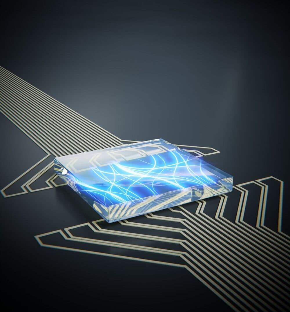
What are the potential uses for molecular machines, which have won the 2016 Nobel Prize in Chemistry.
Category: nanotechnology – Page 284
Though they’re touted as ideal for electronics, two-dimensional materials like graphene may be too flat and hard to stretch to serve in flexible, wearable devices. “Wavy” borophene might be better, according to Rice University scientists.
The Rice lab of theoretical physicist Boris Yakobson and experimental collaborators observed examples of naturally undulating, metallic borophene, an atom-thick layer of boron, and suggested that transferring it onto an elastic surface would preserve the material’s stretchability along with its useful electronic properties.
Highly conductive graphene has promise for flexible electronics, Yakobson said, but it is too stiff for devices that also need to stretch, compress or even twist. But borophene deposited on a silver substrate develops nanoscale corrugations. Weakly bound to the silver, it could be moved to a flexible surface for use.
(Phys.org)—Researchers have used the pressure of light—also called optical forces or sometimes “tractor beams”—to create a new type of rewritable, dynamic 3D holographic material. Unlike other 3D holographic materials, the new material can be rapidly written and erased many times, and can also store information without using any external energy. The new material has potential applications in 3D holographic displays, large-scale volumetric data storage devices, biosensors, tunable lasers, optical lenses, and metamaterials.
The research was conducted by a multidisciplinary team led by Yunuen Montelongo at Imperial College London and Ali K. Yetisen at Harvard University and MIT. In recent papers published in Nature Communications and Applied Physics Letters, the researchers demonstrated the reversible optical manipulation of nanostructured materials, which they used to fabricate active 3D holograms, lenses, and memory devices.
The key to creating the 3D holographic material with these advantages was to use optical forces to reversibly modify the material’s properties. The optical forces are produced by the interference of two or more laser beams, which creates an optical pressure capable of moving nanoscale structures. So far, optical forces have mainly been used for just one application: optical tweezers, which can hold and move tiny objects and are mostly used in biological applications.
Smarter thread
Posted in biotech/medical, chemistry, computing, health, mobile phones, nanotechnology
I never get tired in circuitry thread and any new findings.
Tufts University engineers say that revolutionary health diagnostics may be hanging on a thread—one of many threads they have created that integrate nano-scale sensors, electronics and microfluidics into threads ranging from simple cotton to sophisticated synthetics. “We think thread-based devices could potentially be used as smart sutures for surgical implants, smart bandages to monitor wound healing, or integrated with textile or fabric as personalized health monitors and point-of-care diagnostics,” says Sameer Sonkusale, Ph.D., director of the interdisciplinary Nano Lab in the Department of Electrical and Computer Engineering at Tufts School of Engineering, Medford/Somerville, Mass.
Researchers dipped a variety of conductive threads in physical and chemical sensing compounds and connected them to wireless electronic circuitry. The threads, sutured into tissues of rats, collected data on tissue health (pressure, stress, strain and temperature), pH and glucose levels. The data helps determine how wounds are healing, whether infection is emerging or whether the body’s chemistry is out of balance. Thread’s natural wicking properties draw fluids to the sensing compounds. Resulting data is transmitted wirelessly to a cell phone and computer.
To date, substrates for implantable devices have been two-dimensional, expensive and difficult to process, making them suitable for flat tissue, such as skin, but not for organs. “By contrast, thread is abundant, inexpensive, thin and flexible, and can be easily manipulated into complex shapes,” says Pooria Mostafalu, Ph.D., postdoctoral research fellow with the Harvard-MIT Division of Health Sciences and Technology and former Tufts doctoral student.
In 2009, Carbon nanotube tethers with a strength of 9 N/Tex [9 million newton meters/kg] is over twice as strong as any fibers ever produced before.
In 2016, Jian Nong Wang and his colleagues made nanotubes with a process akin to glass blowing: Using a stream of nitrogen gas, they injected ethanol, with a small amount of ferrocene and thiophene added as catalysts, into a 50-mm-wide horizontal tube placed in furnace at 1,150–1,130 °C.
They packed the nanotubes even more densely by pressing the film repeatedly between two rollers.
Nice POV read.
We know that emerging innovations within cutting-edge science and technology (S&T) areas carry the potential to revolutionize governmental structures, economies, and life as we know it. Yet, others have argued that such technologies could yield doomsday scenarios and that military applications of such technologies have even greater potential than nuclear weapons to radically change the balance of power. These S&T areas include robotics and autonomous unmanned system; artificial intelligence; biotechnology, including synthetic and systems biology; the cognitive neurosciences; nanotechnology, including stealth meta-materials; additive manufacturing (aka 3D printing); and the intersection of each with information and computing technologies, i.e., cyber-everything. These concepts and the underlying strategic importance were articulated at the multi-national level in NATO’s May 2010 New Strategic Concept paper: “Less predictable is the possibility that research breakthroughs will transform the technological battlefield … The most destructive periods of history tend to be those when the means of aggression have gained the upper hand in the art of waging war.”
As new and unpredicted technologies are emerging at a seemingly unprecedented pace globally, communication of those new discoveries is occurring faster than ever, meaning that the unique ownership of a new technology is no longer a sufficient position, if not impossible. They’re becoming cheaper and more readily available. In today’s world, recognition of the potential applications of a technology and a sense of purpose in exploiting it are far more important than simply having access to it.
While the suggestions like those that nanotechnology will enable a new class of weapons that will alter the geopolitical landscape remain unrealized, a number of unresolved security puzzles underlying emerging technologies have implications for international security, defense policy, deterrence, governance, and arms control regimes.
Whether for use in safe data encryption, ultrafast calculation of huge data volumes or so-called quantum simulation of highly complex systems: Optical quantum computers are a source of hope for tomorrow’s computer technology. For the first time, scientists now have succeeded in placing a complete quantum optical structure on a chip, as outlined Nature Photonics. This fulfills one condition for the use of photonic circuits in optical quantum computers.
“Experiments investigating the applicability of optical quantum technology so far have often claimed whole laboratory spaces,” explains Professor Ralph Krupke of the KIT. “However, if this technology is to be employed meaningfully, it must be accommodated on a minimum of space.” Participants in the study were scientists from Germany, Poland, and Russia under the leadership of Professors Wolfram Pernice of the Westphalian Wilhelm University of Münster (WWU) and Ralph Krupke, Manfred Kappes, and Carsten Rockstuhl of the Karlsruhe Institute of Technology (KIT).
The light source for the quantum photonic circuit used by the scientists for the first time were special nanotubes made of carbon. They have a diameter 100,000 times smaller than a human hair, and they emit single light particles when excited by laser light. Light particles (photons) are also referred to as light quanta. Hence the term “quantum photonics.”
Researchers at the Karlsruhe Institute of Technology say they have developed a quantum photonic circuit with an electrically driven light source. Described as a ‘complete quantum optical structure on a chip’, the development is said to fulfil one condition for the use of photonic circuits in optical quantum computers.
“Experiments investigating the applicability of optical quantum technology have often claimed whole laboratory spaces,” said Professor Ralph Krupke. “However, if this technology is to be employed meaningfully, it must be accommodated on a minimum of space.”
The light source for the quantum photonic circuit is carbon nanotubes which emit single particles of light when excited by a laser. Because they emit single photons, carbon nanotubes are attractive as light sources for optical quantum computers.
In a perspective article published Sept. 26 online in the Proceedings of the National Academy of Sciences, a team of scientists at UT Dallas’ Alan G. MacDiarmid NanoTech Institute describes the path to developing a new class of artificial muscles made from highly twisted fibers of various materials, ranging from exotic carbon nanotubes to ordinary nylon thread and polymer fishing line.
Because the artificial muscles can be made in different sizes and configurations, potential applications range from robotics and prosthetics to consumer products such as smart textiles that change porosity and shape in response to temperature.
“We call these actuating fibers ‘artificial muscles’ because they mimic the fiber-like form-factor of natural muscles,” said Dr. Carter Haines, associate research professor in the NanoTech Institute and co-lead author of the PNAS article, with research associate Dr. Na Li. “While the name evokes the idea of humanoid robots, we are very excited about their potential use for other practical applications, such as in next-generation intelligent textiles.” Science Based on Ancient Art.