Interaction between glass spheres suspended in a vacuum might one day lead to advances in quantum computing.

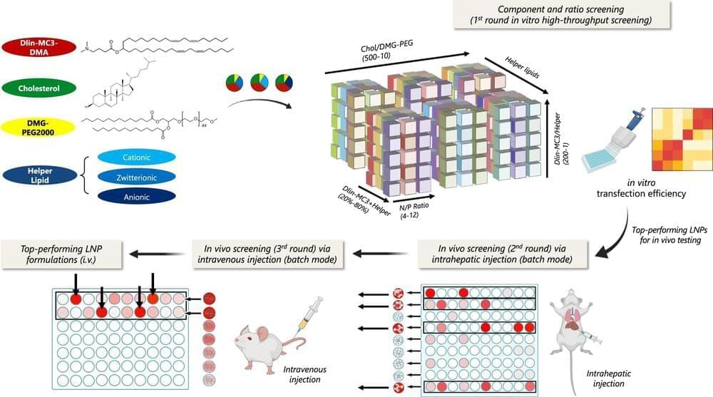
The success of COVID-19 vaccines is a great example of gene medicine’s tremendous potential to prevent viral infections. One reason for the vaccines’ success is their use of lipid nanoparticles, or LNPs, to carry delicate messenger RNA to cells to generate and boost immunity. LNPs—tiny fat particles—have become increasingly popular as a carrier to deliver various gene-based medicines to cells, but their use is complicated because each LNP must be tailored specifically for the therapeutic payload it carries.
A team led by Hai-Quan Mao, a Johns Hopkins materials scientist, has created a platform that shows promise to speed up the LNP design process and make it more affordable. The new approach also can be adapted to other gene therapies.
“In a nutshell, what we have done is creating a method that screens lipid nanoparticle components and their proportions to quickly help identify and create the optimal design for use with various therapeutic genes,” said Mao, director of the Institute for NanoBioTechnology at Johns Hopkins Whiting School of Engineering and professor in the departments of Materials Science and Engineering and Biomedical Engineering.
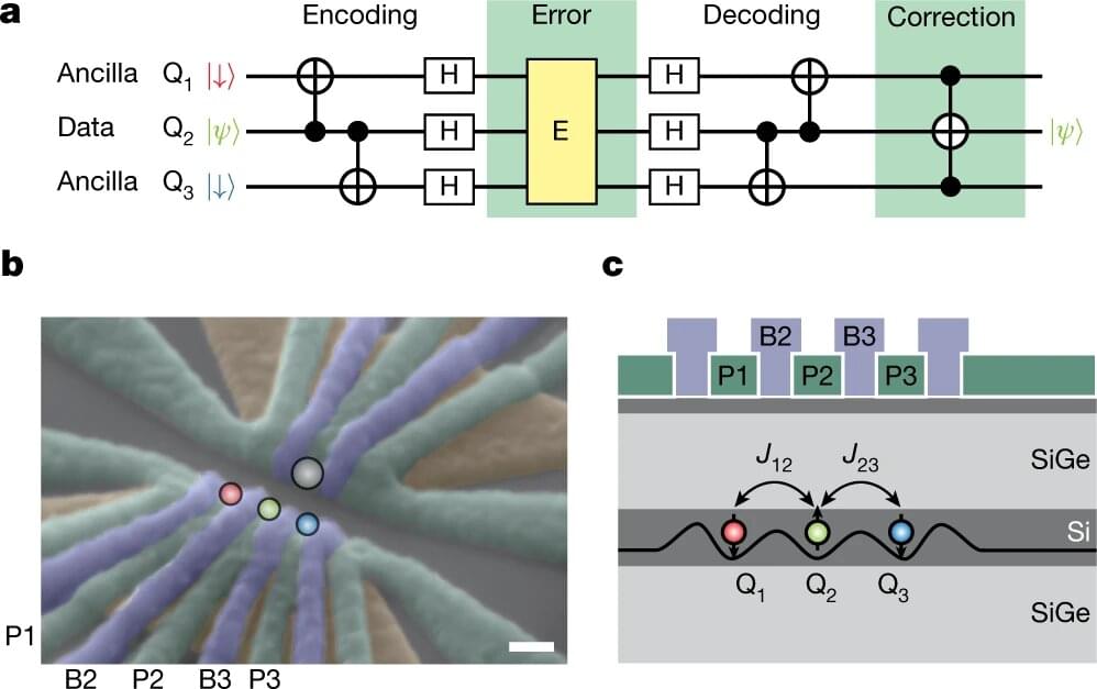
Researchers from RIKEN in Japan have achieved a major step toward large-scale quantum computing by demonstrating error correction in a three-qubit silicon-based quantum computing system. This work, published in Nature, could pave the way toward the achievement of practical quantum computers.
Quantum computers are a hot area of research today, as they promise to make it possible to solve certain important problems that are intractable using conventional computers. They use a completely different architecture, using superimposition states found in quantum physics rather than the simple 1 or 0 binary bits used in conventional computers. However, because they are designed in a completely different way, they are very sensitive to environmental noise and other issues, such as decoherence, and require error correction to allow them to do precise calculations.
One important challenge today is choosing what systems can best act as “qubits”—the basic units used to make quantum calculations. Different candidate systems have their own strengths and weaknesses. Some of the popular systems today include superconducting circuits and ions, which have the advantage that some form of error correction has been demonstrated, allowing them to be put into actual use albeit on a small scale. Silicon-based quantum technology, which has only begun to be developed over the past decade, is known to have an advantage in that it utilizes a semiconductor nanostructure similar to what is commonly used to integrate billions of transistors in a small chip, and therefore could take advantage of current production technology.
In recent years, roboticists have developed a wide variety of robotic systems with different body structures and capabilities. Most of these robots are either made of hard materials, such as metals, or soft materials, such as silicon and rubbery materials.
Researchers at Hong Kong University (HKU) and Lawrence Berkeley National Laboratory have recently created Aquabots, a new class of soft robots that are predominantly made of liquids. As most biological systems are predominantly made up of water or other aqueous solutions, the new robots, introduced in a paper published in ACS Nano, could have highly valuable biomedical and environmental applications.
“We have been engaged in the development of adaptive interfacial assemblies of materials at the oil-water and water-water interface using nanoparticles and polyelectrolytes,” Ho Cheung (Anderson) Shum, Thomas P. Russell, and Shipei Zhu told TechXplore via email. “Our idea was to assemble the materials that the interface and the assemblies lock in the shapes of the liquids. The shapes are dictated using external forces to generate arbitrary shapes or to use all-liquid 3D printing to be able to spatially organize the assemblies.”

Constructing a tiny robot out of DNA
DNA, or deoxyribonucleic acid, is a molecule composed of two long strands of nucleotides that coil around each other to form a double helix. It is the hereditary material in humans and almost all other organisms that carries genetic instructions for development, functioning, growth, and reproduction. Nearly every cell in a person’s body has the same DNA. Most DNA is located in the cell nucleus (where it is called nuclear DNA), but a small amount of DNA can also be found in the mitochondria (where it is called mitochondrial DNA or mtDNA).
By scientists from Inserm, CNRS, and Université de Montpellier at the Structural Biology Center in Montpellier. The nano-robot could lead to a closer study of the mechanical forces applied at microscopic levels, which are important for various biological and pathological processes.
The study was published in Nature Communications.
Cellular Mechanosensitivity
A novel method for measuring nanoparticle size could have applications in industry and basic materials science research.
Nanoparticles are present in everything from paints to pharmaceutical products. While nanoparticles have many important characteristics, such as molecular composition and shape, it is their size that determines many chemical and physical properties. A new technique relying on an optical vortex—a laser beam whose wave fronts twist around a dark central region—allows researchers to characterize nanoparticle size rapidly and continuously [1]. This light-based size probe might one day find applications in numerous industrial settings and aid fundamental materials science research.
It is difficult to precisely synthesize nanoparticles with the desired dimensions, so manufacturers must often validate that their nanoparticles have the right size to comply with regulations and to ensure product quality. There are many ways of determining nanoparticle size, but one popular approach, dynamic light scattering (DLS), is based on measurements of Brownian motion, the random particle movement caused by jostling from the surrounding liquid medium. In DLS, the Brownian motion is determined by measuring fluctuations in laser light scattering from the nanoparticles. In general, the faster the Brownian motion, the smaller the particles. But current techniques are generally not capable of characterizing the largest particles and measuring them continuously.
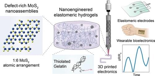
Flexible electronics have enabled the design of sensors, actuators, microfluidics and electronics on flexible, conformal and/or stretchable sublayers for wearable, implantable or ingestible applications. However, these devices have very different mechanical and biological properties when compared to human tissue and thus cannot be integrated with the human body.
A team of researchers at Texas A&M University has developed a new class of biomaterial inks that mimic native characteristics of highly conductive human tissue, much like skin, which are essential for the ink to be used in 3D printing.
This biomaterial ink leverages a new class of 2D nanomaterials known as molybdenum disulfide (MoS2). The thin-layered structure of MoS2 contains defect centers to make it chemically active and, combined with modified gelatin to obtain a flexible hydrogel, comparable to the structure of Jell-O.