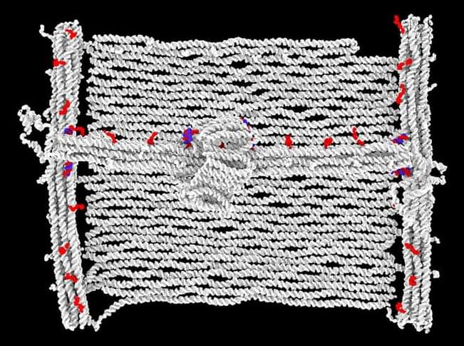
A nanoscale machine made from DNA moves under external control and prints by selectively modifying pixels on a canvas.


Using nanotechnology, scientists have created a newly designed neuromorphic electronic device that endows microrobotics with colorful vision.
Researchers at Georgia State University have successfully designed a new type of artificial vision device that incorporates a novel vertical stacking architecture and allows for greater depth of color recognition and micro-level scaling. The new research study was published on April 18, 2022, in the top journal ACS Nano.
“This work is the first step toward our final destination–to develop a micro-scale camera for microrobots,” says assistant professor of Physics Sidong Lei, who led the research. “We illustrate the fundamental principle and feasibility to construct this new type of image sensor with emphasis on miniaturization.”


A large team of researchers at the University of Washington, working with colleagues from Université Montpellier and the Fred Hutchinson Cancer Research Center, has taken a major step toward the creation of an axle-rotor nanomachine. In their paper published in the journal Science, the group describes how they used DNA coding to customize E. coli to push them into creating proteins that assembled into rotors and axles.
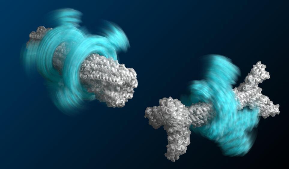
A large team of researchers at the University of Washington, working with colleagues from Université Montpellier and the Fred Hutchinson Cancer Research Center, has taken a major step toward the creation of an axle-rotor nanomachine. In their paper published in the journal Science, the group describes how they used DNA coding to customize E. coli to push them into creating proteins that assembled into rotors and axles.
As the researchers note, molecular engines are abundant in nature, from the tails of flagellum on some bacteria to the F1 motor of ATPase. And while such examples have served as good models, attempts to harness them in nature or to create new ones in the lab have been mostly unsuccessful. This is due to the single purpose features of natural engines and the unpredictability of protein folding in synthetic attempts. In this new effort, the researchers have overcome some of the hurdles that others have faced and have taken a major step toward the creation of a molecular engine by creating two of the main parts necessary for such a device—an axle and a rotor—and even managed to connect them to each other.
To create their engine parts, the researchers first used a software program called Rosetta that allowed them to design ring-like proteins with specified diameters. They then used the data from the program to add DNA coding to amino acids in E. coli bacteria that make up proteins. Such proteins are made of chains of the amino acids—it is the sequence of them that defines the shape they will take when they spontaneously fold. The team was able to coax some of the proteins into folding into rotor shapes and others into axle shapes. They then went further by coaxing multiple proteins to fold together into rotor-axle combinations—the rudimentary parts necessary for a molecular engine.
Bart Blommaertsif it helps. But don’t cut internet cables with that thing!!
Andreas StürmerFinally. Is it going to be a rail or car tunnel?
Eric KlienAdmin.
Andreas Stürmer Rail.
Jose Ruben Rodriguez Fuentes shared a link.
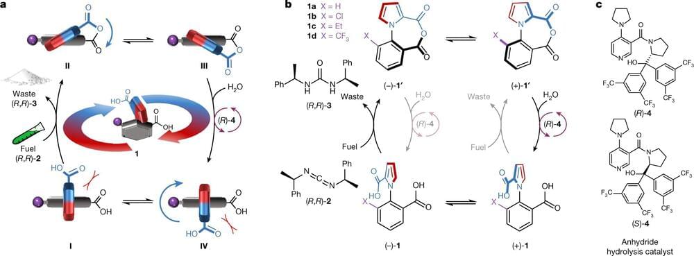
A team of researchers at the University of Manchester has created a molecular motor that consumes chiral fuel to drive rotation around a single covalent bond. In their paper published in the journal Nature, the group describes their work in developing a chemically powered directionally rotating motor and why they believe their efforts will result in similar systems being developed with other materials.
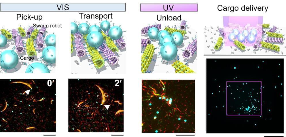
In a global first, scientists have demonstrated that molecular robots are able to accomplish cargo delivery by employing a strategy of swarming, achieving a transport efficiency five times greater than that of single robots.
Swarm robotics is a new discipline, inspired by the cooperative behavior of living organisms, that focuses on the fabrication of robots and their utilization in swarms to accomplish complex tasks. A swarm is an orderly collective behavior of multiple individuals. Macro-scale swarm robots have been developed and employed for a variety of applications, such as transporting and accumulating cargo, forming shapes, and building complex structures.
A team of researchers, led by Dr. Mousumi Akter and Associate Professor Akira Kakugo from the Faculty of Science at Hokkaido University, has succeeded in developing the world’s first working micro-sized machines utilizing the advantages of swarming. The findings were published in the journal Science Robotics. The team included Assistant Professor Daisuke Inoue, Kyushu University; Professor Henry Hess, Columbia University; Professor Hiroyuki Asanuma, Nagoya University; and Professor Akinori Kuzuya, Kansai University.
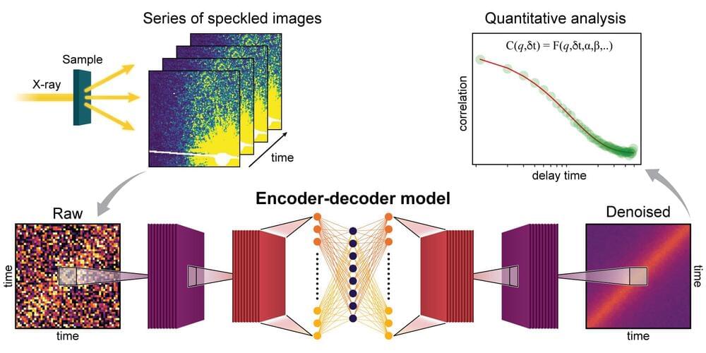
Scientists from the National Synchrotron Light Source II (NSLS-II) and Computational Science Initiative (CSI) at the U.S. Department of Energy’s (DOE) Brookhaven National Laboratory have helped to solve a common problem in synchrotron X-ray experiments: reducing the noise, or meaningless information, present in data. Their work aims to improve the efficiency and accuracy of X-ray studies at NSLS-II, with the goal of enhancing scientists’ overall research experience at the facility.
NSLS-II, a DOE Office of Science user facility, produces X-ray beams for the study of a huge variety of samples, from potential new battery materials to plants that can remediate contaminated soil. Researchers from across the nation and around the globe come to NSLS-II to investigate their samples using X-rays, collecting huge amounts of data in the process. One of the many X-ray techniques available at NSLS-II to visiting researchers is X-ray photon correlation spectroscopy (XPCS). XPCS is typically used to study material behaviors that are time-dependent and take place at the nanoscale and below, such as the dynamics between and within structural features, like tiny grains. XPCS has been used, for example, to study magnetism in advanced computing materials and structural changes in polymers (plastics).
While XPCS is a powerful technique for gathering information, the quality of the data collected and range of materials that can be studied is limited by the “flux” of the XPCS X-ray beam. Flux is a measure of the number of X-rays passing through a given area at a point in time, and high flux can lead to too much “noise” in the data, masking the signal the scientists are seeking. Efforts to reduce this noise have been successful for certain experimental setups. But for some types of XPCS experiments, achieving a more reasonable signal-to-noise ratio is a big challenge.
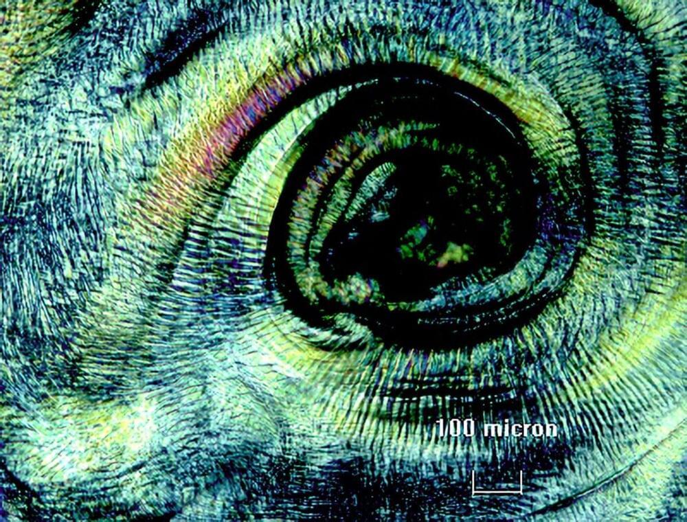
Nature may abhor a vacuum, but it sure loves structure. Complex, self-organized assemblies are found throughout the natural world, from double-helix DNA molecules to the photonic crystals that make butterfly wings so colorful and iridescent.
A Cornell-led project has created synthetic nanoclusters that can mimic this hierarchical self-assembly all the way from the nanometer to the centimeter scale, spanning seven orders of magnitude. The resulting synthetic thin films have the potential to serve as a model system for exploring biomimetic hierarchical systems and future advanced functions.
This image shows synthetic nanoparticles as they self-organize into filaments, then twist into cables, then bundle together into highly ordered bands, ultimately resulting in a thin film that is patterned at centimeter scales. (Image courtesy of the researchers)