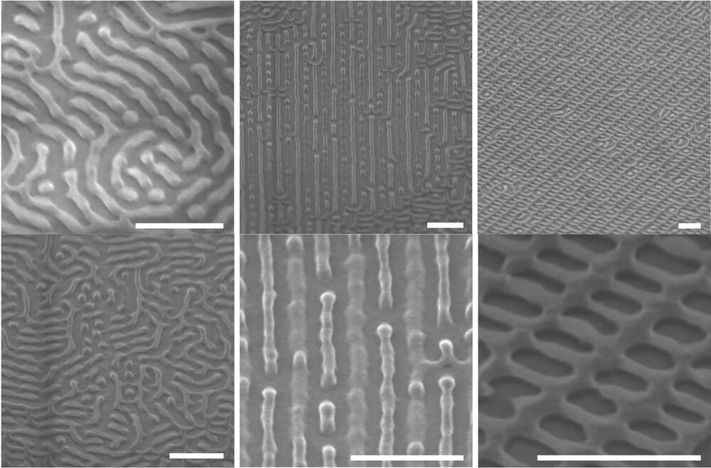
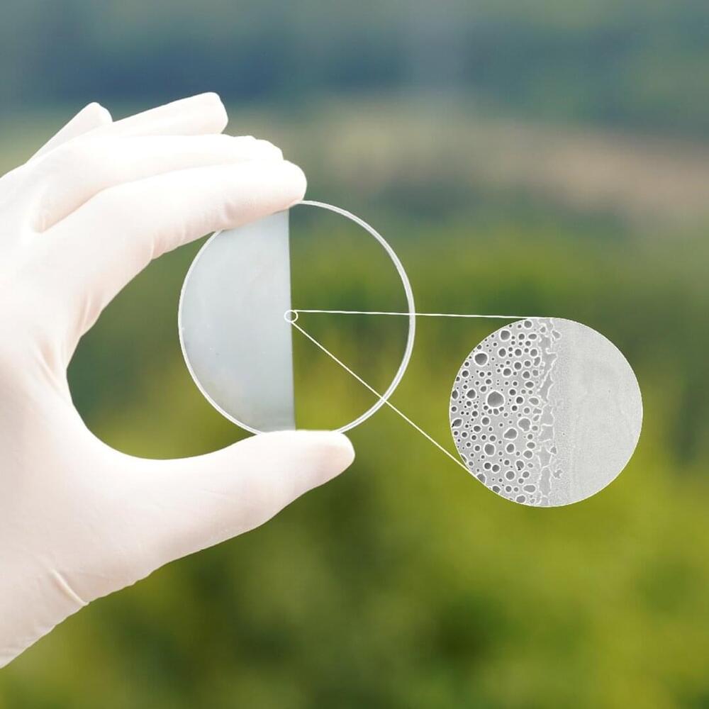
Antibiotic resistance is a global human health threat, causing routine treatments of bacterial infections to become increasingly difficult. The problem is exacerbated by biofilm formation by bacterial pathogens on the surfaces of indwelling medical and dental devices that facilitate high levels of tolerance to antibiotics. The development of new antibacterial nanostructured surfaces shows excellent prospects for application in medicine as next-generation biomaterials. The physico-mechanical interactions between these nanostructured surfaces and bacteria lead to bacterial killing or prevention of bacterial attachment and subsequent biofilm formation, and thus are promising in circumventing bacterial infections. This Review explores the impact of surface roughness on the nanoscale in preventing bacterial colonization of synthetic materials and categorizes the different mechanisms by which various surface nanopatterns exert the necessary physico-mechanical forces on the bacterial cell membrane that will ultimately result in cell death.
Category: nanotechnology – Page 194
Nature has spent millennia honing the virus into a ruthlessly efficient delivery vehicle for nucleic acids. Viruses have even been harnessed for our own delivery purposes. But some applications have had only mixed success. For example, commercial applications of genetic engineering, which require high scalability, low cost, and impeccable safety, remain a challenge.
Although they can easily enter the body and inject their payload into cells, viruses may stimulate a dangerous immune reaction and cause long-term medical complications. In addition, viruses can be expensive and time consuming to cultivate.
Safer and more practical alternatives to viruses are being sought by innovative companies. For example, these companies are developing nonviral gene delivery systems that incorporate nanoparticle formulations, ultrasound, and electric fields. These systems can slip bits of genetic material into cells efficiently and cost-effectively in a range of applications.
Brian Wang is a Futurist Thought Leader and a popular Science blogger with 1 million readers per month. His blog Nextbigfuture.com is ranked #1 Science News Blog. It covers many disruptive technology and trends including Space, Robotics, Artificial Intelligence, Medicine, Anti-aging Biotechnology, and Nanotechnology.
Known for identifying cutting edge technologies, he is currently a Co-Founder of a startup and fundraiser for high potential early-stage companies. He is the Head of Research for Allocations for deep technology investments and an Angel Investor at Space Angels.
A frequent speaker at corporations, he has been a TEDx speaker, a Singularity University speaker and guest at numerous interviews for radio and podcasts. He is open to public speaking and advising engagements.
MIT engineers have developed a novel platform for the controlled delivery of certain important drugs, nutrients, and other substances to human cells.
In work that could impact industries from pharmaceuticals to cosmetics, MIT engineers have developed a platform for the controlled delivery of drugs and more to human cells. The simple approach creates capsules containing nanoscale droplets loaded with an active ingredient.
California company NDB says its nano-diamond batteries will absolutely upend the energy equation, acting like tiny nuclear generators. They will blow any energy density comparison out of the water, lasting anywhere from a decade to 28,000 years without ever needing a charge. They will offer higher power density than lithium-ion. They will be nigh-on indestructible and totally safe in an electric car crash. And in some applications, like electric cars, they stand to be considerably cheaper than current lithium-ion packs despite their huge advantages.
The heart of each cell is a small piece of recycled nuclear waste. NDB uses graphite nuclear reactor parts that have absorbed radiation from nuclear fuel rods and have themselves become radioactive. Untreated, it’s high-grade nuclear waste: dangerous, difficult and expensive to store, with a very long half-life.
This graphite is rich in the carbon-14 radioisotope, which undergoes beta decay into nitrogen, releasing an anti-neutrino and a beta decay electron in the process. NDB takes this graphite, purifies it and uses it to create tiny carbon-14 diamonds. The diamond structure acts as a semiconductor and heat sink, collecting the charge and transporting it out. Completely encasing the radioactive carbon-14 diamond is a layer of cheap, non-radioactive, lab-created carbon-12 diamond, which contains the energetic particles, prevents radiation leaks and acts as a super-hard protective and tamper-proof layer.
In Korea, scientists are turning to better ways for improving our screen time, and this means 3D printing something most of us know little about: quantum dots. Focusing on refining the wonders of virtual reality and other electronic displays even further, researchers from the Nano Hybrid Technology Research Center of Korea Electrotechnology Research Institute (KERI), a government-funded research institute under National Research Council of Science & Technology (NST) of the Ministry of Science and ICT (MSIT), have created nanophotonic 3D printing technology for screens. Meant to be used with virtual reality, as well as TVs, smartphones, and wearables, high resolution is achieved due to a 3D layout expanding the density and quality of the pixels.
Led by Dr. Jaeyeon Pyo and Dr. Seung Kwon Seol, the team has published the results of their research and development in “3D-Printed Quantum Dot Nanopixels.” While pixels are produced to represent data in many electronics, conventionally they are created with 2D patterning. To overcome limitations in brightness and resolution, the scientists elevated this previously strained technology to the next level with 3D printed quantum dots to be contained within polymer nanowires.
Researchers have fashioned ultrathin silicon nanoantennas that trap and redirect light, for applications in quantum computing, LIDAR and even the detection of viruses.
Light is notoriously fast. Its speed is crucial for rapid information exchange, but as light zips through materials, its chances of interacting and exciting atoms and molecules can become very small. If scientists can put the brakes on light particles, or photons, it would open the door to a host of new technology applications.
Now, in a paper published on August 17, 2020, in Nature Nanotechnology, Stanford scientists demonstrate a new approach to slow light significantly, much like an echo chamber holds onto sound, and to direct it at will. Researchers in the lab of Jennifer Dionne, associate professor of materials science and engineering at Stanford, structured ultrathin silicon chips into nanoscale bars to resonantly trap light and then release or redirect it later. These “high-quality-factor” or “high-Q” resonators could lead to novel ways of manipulating and using light, including new applications for quantum computing, virtual reality and augmented reality; light-based WiFi; and even the detection of viruses like SARS-CoV-2.
Light is notoriously fast. Its speed is crucial for rapid information exchange, but as light zips through materials, its chances of interacting and exciting atoms and molecules can become very small. If scientists can put the brakes on light particles, or photons, it would open the door to a host of new technology applications.
Now, in a paper published on Aug. 17, in Nature Nanotechnology, Stanford scientists demonstrate a new approach to slow light significantly, much like an echo chamber holds onto sound, and to direct it at will. Researchers in the lab of Jennifer Dionne, associate professor of materials science and engineering at Stanford, structured ultrathin silicon chips into nanoscale bars to resonantly trap light and then release or redirect it later. These “high-quality-factor” or “high-Q” resonators could lead to novel ways of manipulating and using light, including new applications for quantum computing, virtual reality and augmented reality; light-based WiFi; and even the detection of viruses like SARS-CoV-2.
“We’re essentially trying to trap light in a tiny box that still allows the light to come and go from many different directions,” said postdoctoral fellow Mark Lawrence, who is also lead author of the paper. “It’s easy to trap light in a box with many sides, but not so easy if the sides are transparent—as is the case with many Silicon-based applications.”
Have you ever spilled your coffee on your desk? You may then have observed one of the most puzzling phenomena of fluid mechanics—the coffee ring effect. This effect has hindered the industrial deployment of functional inks with graphene, 2-D materials, and nanoparticles because it makes printed electronic devices behave irregularly.
Now, after studying this process for years, a team of researchers have created a new family of inks that overcomes this problem, enabling the fabrication of new electronics such as sensors, light detectors, batteries and solar cells.
Coffee rings form because the liquid evaporates quicker at the edges, causing an accumulation of solid particles that results in the characteristic dark ring. Inks behave like coffee—particles in the ink accumulate around the edges creating irregular shapes and uneven surfaces, especially when printing on hard surfaces like silicon wafers or plastics.
“For the first time ever, we have direct experimental evidence that an external quantum efficiency above 100% is possible in a single photodiode without any external antireflection,” says Hele Savin, associate professor of Micro and Nanoelectonics at Aalto University in Finland. The results come just a few years after Savin and colleagues at Aalto University demonstrated almost unity efficiency over the wavelength range 250–950 nm in photodiodes made with black silicon, where the silicon surface is nanostructured and coated to suppress losses.
Noticing some curious effects in the UV region, Savin’s group extended their study of the devices to focus on this region of the electromagnetic spectrum. UV sensing has multiple applications, including spectroscopy and imaging, flame detection, water purification and biotechnology. While annual market demand for UV photodiodes is expected to increase to 30%, the efficiency of these devices has been limited to 80% at best. To Savin’s surprise, closer analysis of their device’s response to UV light revealed that the external quantum efficiency could exceed 130%. Independent measurements at Physikalisch Technische Bundesanstalt (PTB) verified the results.