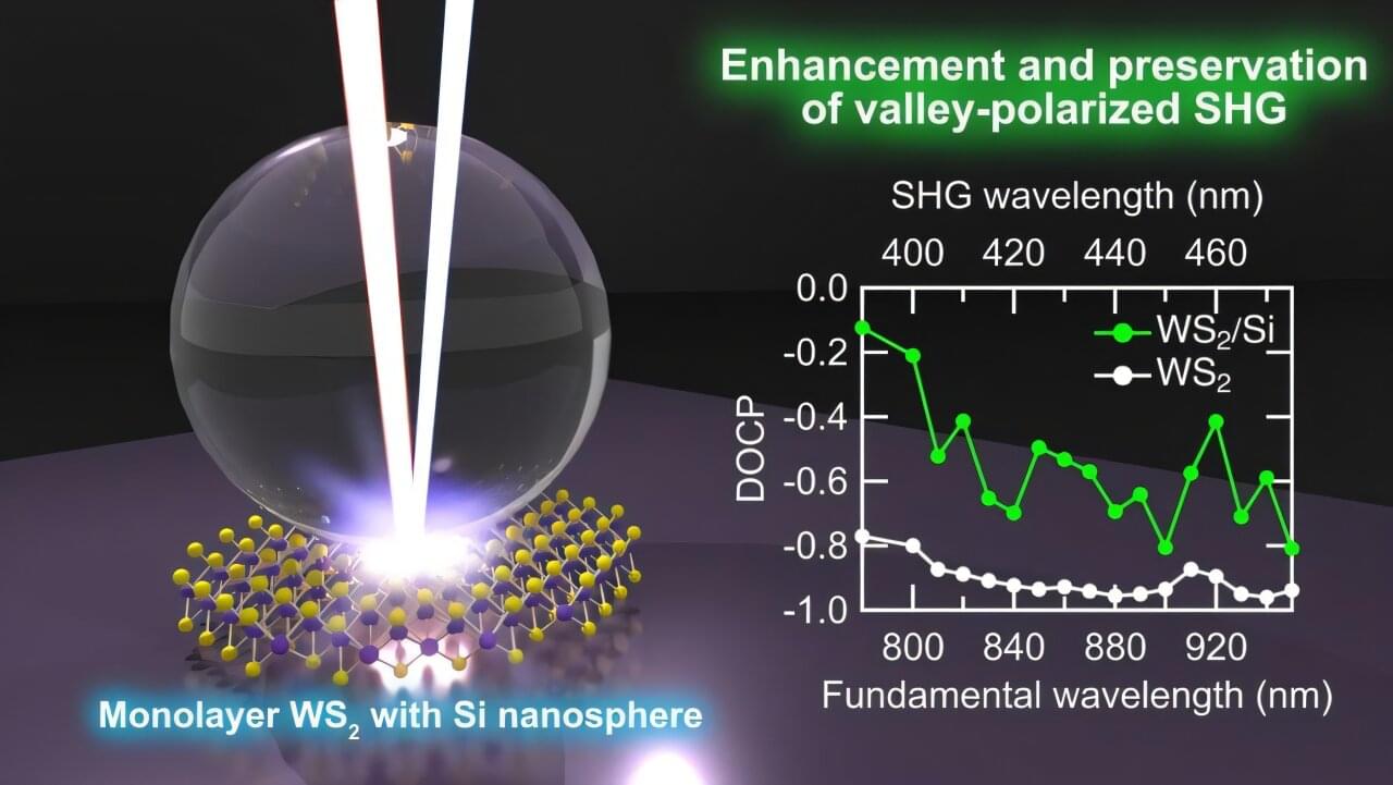
Light can carry angular momentum in two distinct ways. One comes from polarization, which describes how the electric field rotates. The other comes from the shape of the wavefront itself, which can twist like a corkscrew as it travels. This second form, known as orbital angular momentum, has attracted wide interest because it allows light to encode information, interact with matter in new ways, and probe physical and biological systems. Despite this promise, producing well-defined twisted light in free space remains technically challenging, especially when the light originates from small or localized sources.
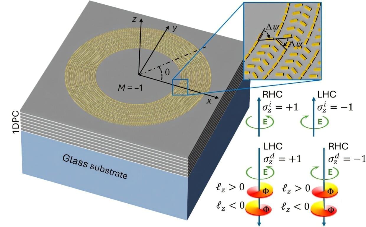
Recent research reported in Advanced Photonics Nexus demonstrates a route to generating twisted light beams by combining a dielectric multilayer with a patterned metallic surface. The work shows that surface-bound light waves can be converted into free-space beams with controlled angular momentum and polarization. Importantly, the approach avoids several limitations of earlier designs and points toward future integration with single-photon emitters.
Many existing methods for generating orbital angular momentum rely on reshaping a laser beam using holograms, liquid-crystal plates, or patterned films known as metasurfaces. While effective for large, externally illuminated beams, these approaches struggle when light must be generated directly on a chip or from nanoscale emitters such as quantum dots or single molecules. Such sources cannot uniformly illuminate a structure or arrive at a precisely defined angle, making efficient beam shaping difficult.

