Link :- https://eng.unimelb.edu.au/ingenium/wearable-device-makes-me…f-a-finger
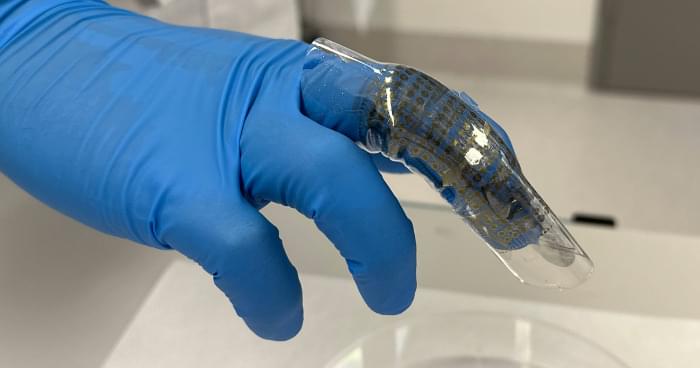
Researchers from the University of Melbourne and RMIT University have invented an experimental wearable device that generates power from a user’s bending finger and can create and store memories, in a promising step towards health monitoring and other technologies.
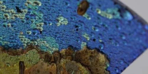
Multifunctional devices normally require several materials in layers, which involves the time-consuming challenge of stacking nanomaterials with high precision. This innovation features a single nanomaterial incorporated into a stretchable casing fitted to a person’s finger. The nanomaterial enables the device to produce power simply through the user bending their finger. The super-thin material also allows the device to perform memory tasks.
The team, led by RMIT University and the University of Melbourne, in collaboration with other Australian and international institutions, made the proof-of-concept device with the rust of a low-temperature liquid metal called bismuth, which is safe and well suited for wearable applications.

