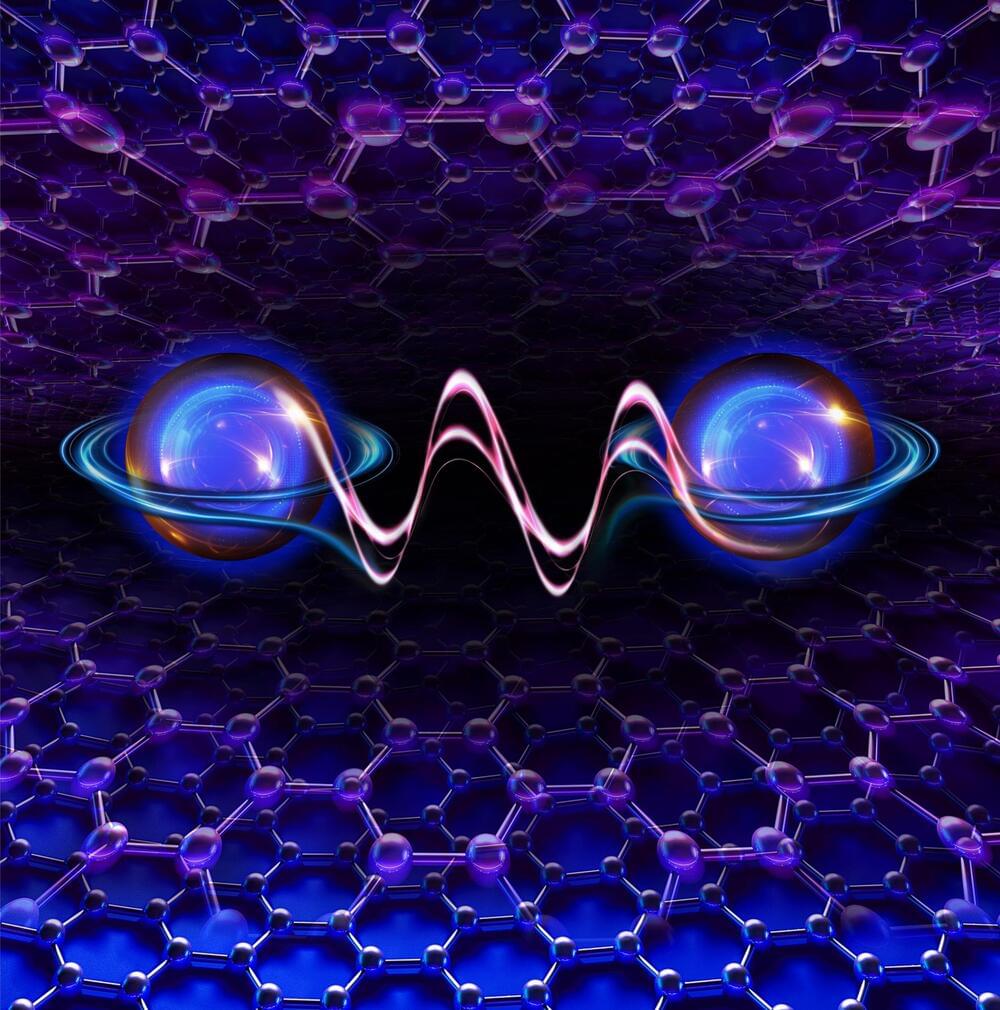
Toggle light / dark theme

A gas made of particles of light, or photons, becomes easier to compress the more you squash it. This strange property could prove useful in making highly sensitive sensors.

While gases are normally made from atoms or molecules, it is possible to create a gas of photons by trapping them with lasers. But a gas made this way doesn’t have a uniform density – researchers say it isn’t homogeneous, or pure – making it difficult to study properly.

Now Julian Schmitt at the University of Bonn, Germany, and his colleagues have made a homogeneous photon gas for the first time by trapping photons between two nanoscale mirrors.

Scientists from the NTU Singapore and the Korea Institute of Machinery & Materials (KIMM) have developed a technique to create a highly uniform and scalable semiconductor wafer, paving the way to higher chip yield and more cost-efficient semiconductors.

Left: Image of a six-inch silicon wafer with printed metal layers and its top-view scanning electron microscope image. Right: Image of the six-inch silicon wafer with nanowires and its cross-sectional scanning electron microscope image. (Image: NTU Singpore)

Semiconductor chips commonly found in smart phones and computers are difficult and complex to make, requiring highly advanced machines and special environments to manufacture.

The microscopic components that make up computer chips must be made at staggering scales. With billions of transistors in a single processor, each made of multiple materials carefully arranged in patterns as thin as a strand of DNA, their manufacturing tools must also operate at a molecular level.

Typically, these tools involve using stencils to selectively pattern or remove materials with high fidelity, layer after layer, to form nanoscale electronic devices. But as chips must fit more and more components to keep up with the digital world’s growing computational demands, these nanopatterning stencils must also become smaller and more precise.

Now, a team of Penn Engineers has demonstrated how a new class of polymers could do just that. In a new study, the researchers demonstrated how “multiblock” copolymers can produce exceptionally ordered patterns in thin films, achieving spacings smaller than three nanometers.

Get a year of Nebula and Curiosity Stream for only $14.79 when you sign up at http://www.curiositystream.com/joescott.
We’ve been hearing for years how nanotechnology is going to change the world. In movies and in headlines, nanotechnology is almost like “future magic” that will make the impossible possible. But how realistic are those predictions? And how close are we to seeing some of them come true? Let’s take a look at the state of nanotechnology.

Want to support the channel? Here’s how:

Patreon: http://www.patreon.com/answerswithjoe.
Channel Memberships: https://www.youtube.com/channel/UC-2YHgc363EdcusLIBbgxzg/join.
T-Shirts & Merch: http://www.answerswithjoe.com/store.

Check out my 2nd channel, Joe Scott TMI:
https://www.youtube.com/channel/UCqi721JsXlf0wq3Z_cNA_Ew.

You can listen to my podcast, Conversations With Joe on Spotify, Apple Podcasts, Google Podcasts, or wherever you get your podcasts.
Spotify 👉 https://spoti.fi/3AWUFAO
Apple Podcasts 👉 https://apple.co/3Hngf3v.
Google Podcasts 👉 https://bit.ly/3s9Sq9b.

Interested in getting a Tesla or going solar? Use my referral link and get discounts and perks:

NASA

That spot of oil on the garage floor dripping from your engine indicates a problem. It’s so small that you put off going to the mechanic, until you hear a new noise and the oil pressure warning light goes off. The bad news is that one of the bearings in the crankshaft is the source of the issue. Due to wear, the normally round part is now more elliptical in shape. Some of the metal has worn away, landing you with a costly repair.

This kind of wear on engine components is common because of friction, and it happens in all machinery with moving parts. Lubricants that reduce friction can only delay and minimize this inevitable damage. The idea of reversing that wear by fixing a worn part was the dream of Washington State University PhD candidate Pavlo “Pasha” Rudenko, who decided to research using smart nanoparticles to replace eroded material.

R/IntelligenceSupernova — dedicated to techno-optimists, singularitarians, transhumanist thinkers, cosmists, futurists, AI researchers, cyberneticists, crypto enthusiasts, VR creators, artists, philosophers of mind. Accelerating now towards the Cybernetic Singularity with unprecedented advances in AI & Cybernetics, VR, Biotechnology, Nanotechnology, Bionics, Genetic Engineering, Optogenetics, Neuroengineering, Robotics, and other IT fields.

Join now: https://www.reddit.com/r/IntelligenceSupernova.

#Subreddit #IntelligenceSupernova

Ever since its discovery in 2004, graphene has received attention owing to its extraordinary properties, among them its extremely high carrier mobility. However, the high carrier mobility has only been observed using techniques that require complex and expensive fabrication methods. Now, researchers at Chalmers report on a surprisingly high charge-carrier mobility of graphene using much cheaper and simpler methods.

“This finding shows that graphene transferred to cheap and flexible substrates can still have an uncompromisingly high mobility, and it paves the way for a new era of graphene nano-electronics,” says Munis Khan, researcher at Chalmers University of Technology.

Graphene is the one-atom-thick layer of carbon atoms, known as the world’s thinnest material. The material has become a popular choice in semiconductor, automotive and optoelectronic industry due to its excellent electrical, chemical, and material properties. One such property is its extremely .

A research team from KTH Royal Institute of Technology and Max Planck Institute of Colloids and Interfaces reports to have found the key to controlled fabrication of cerium oxide mesocrystals. The research is a step forward in tuning nanomaterials that can serve a wide range of uses—including solar cells, fuel catalysts and even medicine.

Mesocrystals are nanoparticles with identical size, shape and crystallographic orientation, and they can be used as to create artificial nanostructures with customized optical, magnetic or electronic properties. In nature, these three-dimensional structures are found in coral, sea urchins and calcite desert rose, for example. Artificially-produced cerium oxide (CeO2) mesocrystals—or nanoceria—are well-known as catalysts, with antioxidant properties that could be useful in pharmaceutical development.

“To be able to fabricate CeO2 mesocrystals in a controlled way, one needs to understand the formation mechanism of these materials,” says Inna Soroka, a researcher in applied at KTH. She says the team used radiation chemistry to reveal for the first time the ceria mesocrystal formation mechanism.