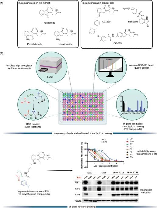
Menu

Blog

Archive for the ‘nanotechnology’ category: Page 159

Oct 9, 2020

Nanobots kill off cancerous tumours as fiction becomes reality

Posted by in categories: biotech/medical, nanotechnology

Circa 2018


Researchers inject tiny devices into the bloodstream to deliver drugs with precision.

Oct 9, 2020

Nanoscale machines convert light into work

Posted by in categories: chemistry, nanotechnology, particle physics

“In previous work, the researchers discovered that when optical matter is exposed to circularly polarized light, it rotates as a rigid body in the direction opposite the polarization rotation. In other words, when the incident light rotates one way the optical matter array responds by spinning the other. This is a manifestation of “negative torque”. The researchers speculated that a machine could be developed based on this new phenomenon.

In the new work, the researchers created an optical matter machine that operates much like a mechanical machine based on interlocking gears. In such machines, when one gear is turned, a smaller interlocking gear will spin in the opposite direction. The optical matter machine uses circularly polarized light from a laser to create a nanoparticle array that acts like the larger gear by spinning in the optical field. This “optical matter gear” converts the circularly polarized light into orbital, or angular, momentum that influences a nearby probe particle to orbit the nanoparticle array (the gear) in the opposite direction.”


Researchers have developed a tiny new machine that converts laser light into work. These optically powered machines self-assemble and could be used for nanoscale manipulation of tiny cargo for applications such as nanofluidics and particle sorting.

Continue reading “Nanoscale machines convert light into work” »

Oct 8, 2020

Optical Matter Machine: Nanoscale Machines Convert Light Into Work

Posted by in categories: nanotechnology, particle physics

Based on optical matter, new machines could be used to move and manipulate tiny particles.

Researchers have developed a tiny new machine that converts laser light into work. These optically powered machines self-assemble and could be used for nanoscale manipulation of tiny cargo for applications such as nanofluidics and particle sorting.

“Our work addresses a long-standing goal in the nanoscience community to create self-assembling nanoscale machines that can perform work in conventional environments such as room temperature liquids,” said research team leader Norbert F. Scherer from the University of Chicago.

Oct 8, 2020

Engineers create nanoparticles that deliver gene-editing tools to specific tissues and organs

Posted by in categories: bioengineering, biotech/medical, chemistry, genetics, nanotechnology, neuroscience

One of the most remarkable recent advances in biomedical research has been the development of highly targeted gene-editing methods such as CRISPR that can add, remove, or change a gene within a cell with great precision. The method is already being tested or used for the treatment of patients with sickle cell anemia and cancers such as multiple myeloma and liposarcoma, and today, its creators Emmanuelle Charpentier and Jennifer Doudna received the Nobel Prize in chemistry.

While is remarkably precise in finding and altering genes, there is still no way to target treatment to specific locations in the body. The treatments tested so far involve removing or immune system T cells from the body to modify them, and then infusing them back into a patient to repopulate the bloodstream or reconstitute an immune response—an expensive and time-consuming process.

Building on the accomplishments of Charpentier and Doudna, Tufts researchers have for the first time devised a way to directly deliver gene-editing packages efficiently across the and into specific regions of the brain, into immune system cells, or to specific tissues and organs in mouse models. These applications could open up an entirely new line of strategy in the treatment of neurological conditions, as well as cancer, infectious disease, and autoimmune diseases.

Oct 7, 2020

The discovery of triplet spin superconductivity in diamonds

Posted by in categories: materials, nanotechnology

Diamonds have a firm foothold in our lexicon. Their many properties often serve as superlatives for quality, clarity and hardiness. Aside from the popularity of this rare material in ornamental and decorative use, these precious stones are also highly valued in industry where they are used to cut and polish other hard materials and build radiation detectors.

More than a decade ago, a new property was uncovered in when high concentrations of boron are introduced to it: superconductivity. Superconductivity occurs when two electrons with opposite spin form a pair (called a Cooper pair), resulting in the electrical resistance of the material being zero. This means a large supercurrent can flow in the material, bringing with it the potential for advanced technological applications. Yet, little work has been done since to investigate and characterize the nature of a diamond’s superconductivity and therefore its potential applications.

New research led by Professor Somnath Bhattacharyya in the Nano-Scale Transport Physics Laboratory (NSTPL) in the School of Physics at the University of the Witwatersrand in Johannesburg, South Africa, details the phenomenon of what is called “triplet superconductivity” in diamond. Triplet superconductivity occurs when electrons move in a composite spin state rather than as a single pair. This is an extremely rare, yet efficient form of superconductivity that until now has only been known to occur in one or two other materials, and only theoretically in diamonds.

Oct 7, 2020

“World’s fastest electrodes” triple the density of lithium batteries

Posted by in categories: energy, nanotechnology

French company Nawa technologies says it’s already in production on a new electrode design that can radically boost the performance of existing and future battery chemistries, delivering up to 3x the energy density, 10x the power, vastly faster charging and battery lifespans up to five times as long.

Nawa is already known for its work in the ultracapacitor market, and the company has announced that the same high-tech electrodes it uses on those ultracapacitors can be adapted for current-gen lithium-ion batteries, among others, to realize some tremendous, game-changing benefits.

Continue reading “‘World’s fastest electrodes’ triple the density of lithium batteries” »

Oct 5, 2020

Inflight fiber printing toward array and 3D optoelectronic and sensing architectures

Posted by in categories: 3D printing, chemistry, nanotechnology, wearables

Scalability and device integration have been prevailing issues limiting our ability in harnessing the potential of small-diameter conducting fibers. We report inflight fiber printing (iFP), a one-step process that integrates conducting fiber production and fiber-to-circuit connection. Inorganic (silver) or organic {PEDOT: PSS [poly(3,4-ethylenedioxythiophene) polystyrene sulfonate]} fibers with 1- to 3-μm diameters are fabricated, with the fiber arrays exhibiting more than 95% transmittance (350 to 750 nm). The high surface area–to–volume ratio, permissiveness, and transparency of the fiber arrays were exploited to construct sensing and optoelectronic architectures. We show the PEDOT: PSS fibers as a cell-interfaced impedimetric sensor, a three-dimensional (3D) moisture flow sensor, and noncontact, wearable/portable respiratory sensors. The capability to design suspended fibers, networks of homo cross-junctions and hetero cross-junctions, and coupling iFP fibers with 3D-printed parts paves the way to additive manufacturing of fiber-based 3D devices with multilatitude functions and superior spatiotemporal resolution, beyond conventional film-based device architectures.

Small-diameter conducting fibers have unique morphological, mechanical, and optical properties such as high aspect ratio, low bending stiffness, directionality, and transparency that set them apart from other classes of conducting, film-based micro/nano structures (1–3). Orderly assembling of thin conducting fibers into an array or three-dimensional (3D) structures upscales their functional performance for device coupling. Developing new strategies to control rapid synthesis, patterning, and integration of these conducting elements into a device architecture could mark an important step in enabling new device functions and electronic designs (4, 5). To date, conducting micro/nanoscaled fibers have been produced and assembled in a number of ways, from transferring of chemically grown nanofibers/wires (6, 7), writing electrohydrodynamically deposited lines (8, 9), to drawing ultralong fibers (10, 11), wet spinning of fibers (12–14), and 2D/3D direct printing (15–18).

Oct 4, 2020

A new technique for the production of plasmonics devices

Posted by in categories: nanotechnology, particle physics

Research laboratories are constantly developing new materials that are expected to exhibit novel properties bound to revolutionize this or that technology. But it’s not enough to simply create these materials; scientists also need to find efficient methods of processing and fine-tuning them.

Moreover, composites are often made via the addition of nanoparticles into a base matrix, which is why it is necessary to find a way of manipulating the location, size, and concentration rate of these particles that would exclude even the smallest deviations that are invisible to the human eye.

Researchers from ITMO University have improved on the technique of local processing of composites based on nanoporous glass with addition of silver and copper. Now, it is possible to predict with high accuracy the optical properties of a plasmonic component during its treatment.

Oct 3, 2020

The Road to Human 2.0

Posted by in categories: 3D printing, biotech/medical, computing, genetics, life extension, nanotechnology, neuroscience, transhumanism

In the coming 2020s, the world of medical science will make some significant breakthroughs. Through brain implants, we will have the capability to restore lost memories.

~ The 2020s will provide us with the computer power to make the first complete human brain simulation. Exponential growth in computation and data will make it possible to form accurate models of every part of the human brain and its 100 billion neurons.

~ The prototype of the human heart was 3D printed in 2019. By the mid- 2020s, customized 3D- printing of major human body organs will become possible. In the coming decades, more and more of the 78 organs in the human body will become printable.

Continue reading “The Road to Human 2.0” »

Oct 2, 2020

Radiation-immune and repairable chips to fabricate durable electronics

Posted by in categories: computing, nanotechnology

To operate safely and reliably in outdoor environments, electronic devices should be resistant to a wide variety of external factors, including radiation. In fact, high-energy radiation can damage several components of field-effect transistors (FETs) commonly used to make electronics, including their superconducting channel, gate oxide and the insulating materials surrounding it (e.g., isolation or substrate oxides).

For several years, research teams worldwide have thus been trying to devise strategies that could make more resistant to radiation. So far, however, this has proved to be highly challenging, and only a few of the techniques proposed in the past have achieved promising results.

Researchers at Peking University, the Chinese Academy of Sciences and Shanghai Tech University have recently fabricated a radiation-hardened and repairable integrated circuit (IC) based on carbon nanotube transistors with ion gel . This IC, first presented in a paper pre-published in Nature Electronics, could be used to build new that are more resistant to high-energy radiation.