Kilgore, P.B., Sha, J., Andersson, J.A. et al. A new generation needle-and adjuvant-free trivalent plague vaccine utilizing adenovirus-5 nanoparticle platform. npj Vaccines 6, 21 (2021). https://doi.org/10.1038/s41541-020-00275-3
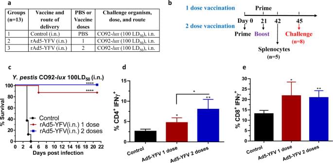
Kilgore, P.B., Sha, J., Andersson, J.A. et al. A new generation needle-and adjuvant-free trivalent plague vaccine utilizing adenovirus-5 nanoparticle platform. npj Vaccines 6, 21 (2021). https://doi.org/10.1038/s41541-020-00275-3
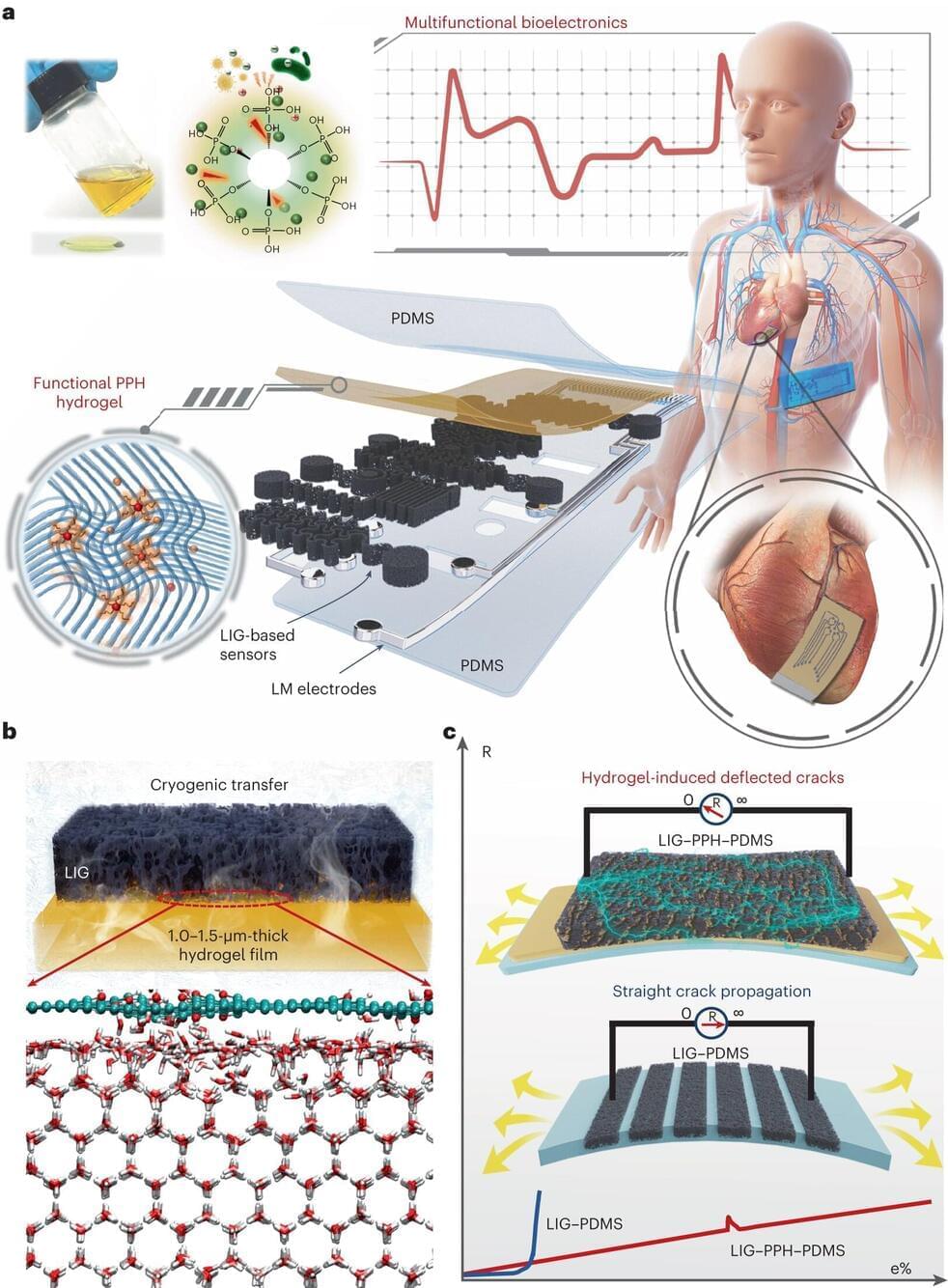
A recent study published in Nature Electronics discusses stretchable graphene–hydrogel interfaces for wearable and implantable bioelectronics.
Stretchable and conductive nanocomposites with mechanically soft, thin and biocompatible features play vital roles in developing wearable skin-like devices, smart soft robots and implantable bioelectronics.
Although several design strategies involving surface engineering have been reported to overcome the mechanical mismatch between the brittle electrodes and stretchable polymers, it is still challenging to realize monolithic integration of various components with diverse functionalities using the current ultrathin stretchable conductive nanocomposites. This is attributed to the lack of suitable conductive nanomaterial systems compatible with facile patterning strategies.

Scientists uncover new insights on polaritons, showing potential for breakthroughs in light manipulation and nanotechnology applications.
An international team of scientists provides an overview of the latest research on light-matter interactions. A team of scientists from the Fritz Haber Institute, the City University of New York, and the Universidad de Oviedo has published a comprehensive review article in the scientific journal Nature Reviews Materials. In this article, they provide an overview of the latest research on polaritons, tiny particles that arise when light and material interact in a special way.
Understanding Polaritons

Producing photons one at a time on demand at room temperature is a key requirement for the rollout of a quantum internet—and the practical quantum computers that would undergird that network. The photons can be used as quantum bits (qubits), the quantum equivalent of classical computing’s 0s and 1s. Labs around the world have devised various ways to generate single photons, but they can involve complex engineering techniques such as doped carbon nanotubes or costly cryogenically-cooled conditions. On the other hand, less complicated techniques such as using traditional light sources do not provide the necessary level of control over single-photon emissions required for quantum networks and computers.
Now, researchers from Tokyo University of Science (TUS) and the Okinawa Institute of Science and Technology have collaborated to develop a prototype room temperature single-photon light source using standard materials and methods. The team described the fabrication of the prototype and its results in a recent issue of the journal Physical Review Applied.
“Our single-photon light source … increases the potential to create quantum networks—a quantum internet—that are cost-effective and accessible.” —Kaoru Sanaka, Tokyo University of Science.

Background: The Promise of Prime Editing
Prime editing is a promising technology for changing genomic deoxyribonucleic acid (DNA) that has the potential to be used to cure genetic diseases in individuals. Prime editors are proteins that can replace a specific deoxyribonucleic acid sequence with another. PE systems necessitate three distinct nucleic acid hybridizations and are not dependent on double-strand deoxyribonucleic acid breaks or donor deoxyribonucleic acid templates.
Researchers must devise efficient and safe techniques to deliver prime editors in tissues in the in vivo settings to fulfill PE’s objective. While viral delivery techniques such as adenoviruses and adeno-associated viruses (AAVs) can transport PE in vivo, non-viral delivery techniques like lipid nanoparticles can sidestep these concerns by packaging PEs as temporarily expressing messenger ribonucleic acids.
Before delving into the prospects of the Fifth Industrial Revolution, let’s reflect on the legacy of its predecessor. The Fourth Industrial Revolution, characterised by the fusion of digital, physical, and biological systems, has already transformed the way we live and work. It brought us AI, blockchain, the Internet of Things, and more. However, it also raised concerns about automation’s impact on employment and privacy, leaving us with a mixed legacy.
The promise of the Fifth Industrial Revolution.
The Fifth Industrial Revolution represents a quantum leap forward. At its core, it combines AI, advanced biotechnology, nanotechnology, and quantum computing to usher in a new era of possibilities. One of its most compelling promises is the extension of human life. With breakthroughs in genetic engineering, regenerative medicine, and AI-driven healthcare, we are inching closer to not just treating diseases but preventing them altogether. It’s a vision where aging is not an inevitability, but a challenge to overcome.
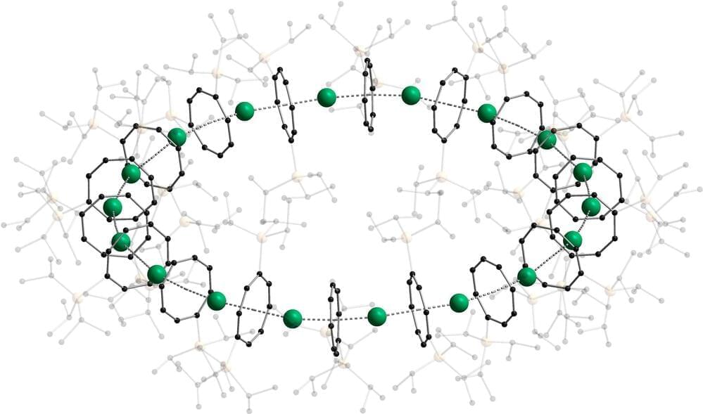
New Compounds for Organometallic Chemistry – Sandwich Complexes in the Form of Rings Are Kept Together by Their Own Energy.
Sandwich compounds are special chemical compounds used as basic building blocks in organometallic chemistry. So far, their structure has always been linear. Recently, researchers of Karlsruhe Institute of Technology (KIT) and the University of Marburg were the first to make stacked sandwich complexes form a nano-sized ring. Physical and other properties of these cyclocene structures will now be further investigated.
Evolution of Sandwich Complexes.
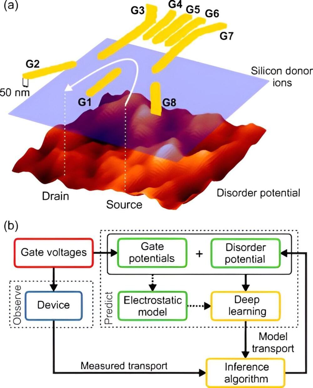
A study led by the University of Oxford has used the power of machine learning to overcome a key challenge affecting quantum devices. For the first time, the findings reveal a way to close the “reality gap”: the difference between predicted and observed behavior from quantum devices. The results have been published in Physical Review X.
Quantum computing could supercharge a wealth of applications, from climate modeling and financial forecasting to drug discovery and artificial intelligence. But this will require effective ways to scale and combine individual quantum devices (also called qubits). A major barrier against this is inherent variability, where even apparently identical units exhibit different behaviors.
Functional variability is presumed to be caused by nanoscale imperfections in the materials from which quantum devices are made. Since there is no way to measure these directly, this internal disorder cannot be captured in simulations, leading to the gap in predicted and observed outcomes.
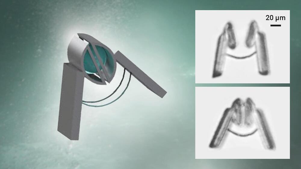
The integration of mechanical memory in the form of springs has for hundreds of years proven to be a key enabling technology for mechanical devices (such as clocks), achieving advanced functionality through complex autonomous movements. Currently, the integration of springs in silicon-based microtechnology has opened the world of planar mass-producible mechatronic devices from which we all benefit, via air-bag sensors for example.
For a new generation of minimally and even non-invasive biomedical applications however, mobile devices that can safely interact mechanically with cells must be achieved at much smaller scales (10 microns) and with much softer forces (pico Newton scale, i.e., lifting weights less than one millionth of a mg) and in customized three-dimensional shapes.
Researchers at the Chemnitz University of Technology, the Shenzhen Institute of Advanced Technology of the Chinese Academy of Sciences and the Leibniz IFW Dresden, in a recent publication in Nature Nanotechnology, have demonstrated that controllable springs can be integrated at arbitrary chosen locations within soft three-dimensional structures using confocal photolithographic manufacturing (with nanoscale precision) of a novel magnetically active material in the form of a photoresist impregnated with customizable densities of magnetic nanoparticles.