Learn about the LVEM5 benchtop electron microscope with TEM, SEM and STEM modes. Nanoscale from your benchtop.
Category: nanotechnology – Page 160
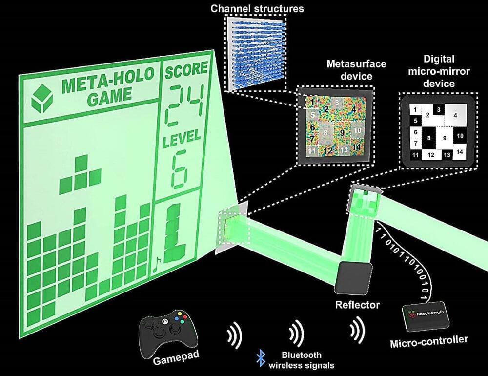
Dynamic interactive bitwise meta-holography with ultra-high computational and display frame rates
Computer-generated holography (CGH) represents a cutting-edge technology that employs computer algorithms to dynamically reconstruct virtual objects. This technology has found extensive applications across diverse fields such as three-dimensional display, optical information storage and processing, entertainment, and encryption.
Despite the broad application spectrum of CGH, contemporary techniques predominantly rely on projection devices like spatial light modulators (SLMs) and digital micromirror devices (DMDs). These devices inherently face limitations in display capabilities, often resulting in narrow field-of-view and multilevel diffraction in projected images.
In recent developments, metasurfaces composed of an array of subwavelength nanostructures have demonstrated exceptional capabilities in modulating electromagnetic waves. By introducing abrupt changes to fundamental wave properties like amplitude and phase through nanostructuring at subwavelength scales, metasurfaces enable modulation effects that are challenging to achieve with traditional devices.
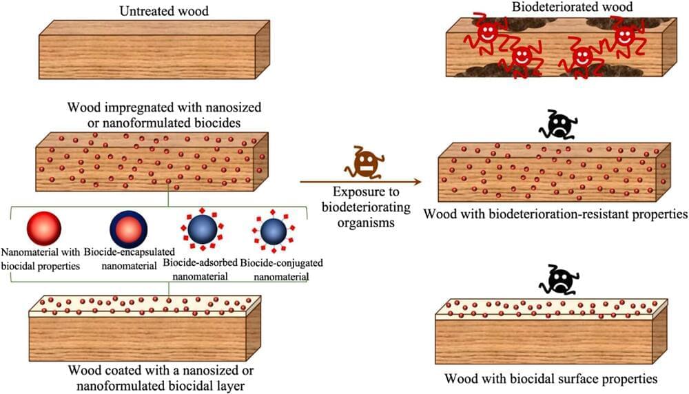
Nanotechnology approaches for creating biodeterioration-resistant wood
Emerging technologies such as nanotechnology can provide efficient approaches by which new materials with broad functions, such as durable and fire-retardant properties, can be developed and subsequently used for the treatment of wood materials.
In a study published in the Journal of Bioresources and Bioproducts, an international team from New Zealand (Scion) and China (Northeast Forestry University) report a review that nanotechnology-based methods can be employed to mitigate these weaknesses and create durable, sustainable wood materials.
These wood nanotechnologies also can be employed to develop wood products with antimicrobial surfaces for various applications. Furthermore, analytical tools used in nanoscience and nanotechnology enable the precise study of wood structure and its components on a nanometer scale, particularly those aspects that can affect wood products’ biodeterioration resistance properties.

Discovery of new material is ‘giant leap’ towards clean energy production and colonisation of Mars
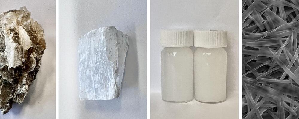
Scientists have developed a new material from a mineral abundant on Mars that they claim could open the door to sustainable habitation on the red planet.
Researchers assessed the potential of a type of nanomaterials – ultrasmall components thousands of times smaller than a human hair – for clean energy production and building materials on Mars.
The study, published in the journal Advanced Functional Materials, found that a material typically considered a waste product by NASA can be altered to provide clean energy and sustainable electronics.
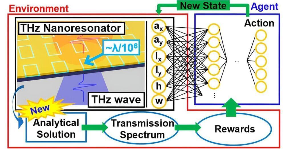
Breakthrough technology amplifies terahertz waves for 6G communication
A team of researchers, led by Professor Hyong-Ryeol Park from the Department of Physics at UNIST has introduced a technology capable of amplifying terahertz (THz) electromagnetic waves by over 30,000 times. This breakthrough, combined with artificial intelligence (AI) based on physical models, is set to revolutionize the commercialization of 6G communication frequencies.
Collaborating with Professor Joon Sue Lee from the University of Tennessee and Professor Mina Yoon from the Oak Ridge National Laboratory, the research team successfully optimized the THz nano-resonator specifically for 6G communication using advanced optimization technology.
The research findings have been published in the online version of Nano Letters.
Direct-to-biology, automated, nano-scale synthesis, and phenotypic screening-enabled E3 ligase modulator discovery
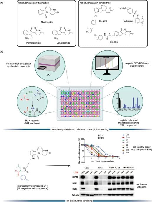
Targeted protein degradation (TPD) is an emerging therapeutic modality and has attracted great attention from academia and industry1,2. The prototypical TPD agents, molecular glues (MGs) and proteolysis targeting chimeras (PROTACs), can lead to temporal proteasomal degradation of the protein-of-interest (POI). PROTACs are small heterobifunctional molecules integrating an E3-ligase binder and a POI binding moiety through a synthetic linker construct. The PROTACs technology has been applied to degrade numerous pathological proteins and a rich pipeline is currently progressing into preclinical and early clinical trials3,4,5. However, overcoming PK/PD issues towards clinical compounds is demanding due to the intrinsically high molecular weight and related physicochemical properties6. On the other hand, MGs are small molecules with beneficial ‘drug-like’ physicochemical properties binding to an E3 ligase, and, similarly to PROTACs, leading to neosubstrate proteasomal degradation. Their mechanism of action is however less predictable; their often hydrophobic surface-exposed portions of the MGs seem to change the hydrophobic surface area of the E3 ligase and thereby leading to neosubstrate ubiquitination and degradation7,8. MGs have already proven their validity as marketed drugs, as there are several approved drugs or clinical compounds working by an MG mechanism (Fig. 1A), for example, the IKZF1/3 degrader thalidomide and its analogs pomalidomide and lenalidomide8, and the RBM39 degrader indisulam9. Thalidomide analogs induce selective ubiquitination and degradation of two lymphoid transcription factors, IKZF1 and IKZF3, by the CRBN-CRL4 ubiquitin ligase10. Additionally, CSNK1A1 (CK1α) was recently discovered as a lenalidomide-specific neo-substrate11. Interestingly, modification of pomalidomide or lenalidomide can have a profound impact on the degradation potency and degradation profiles. For example, CC-220 (Fig. 1A) showed 10-fold more potency in the cells than lenalidomide, and CC-885 (Fig. 1A) was found to induce degradation of the substrate GSPT112,13. Both MGs and PROTACs are emerging drug modalities providing interesting features over classical pharmacology-driven drugs by their ability to drive the destruction of proteins that have multiple functions, thereby potentially overcoming resistance mechanisms and providing new pharmacology. While PROTACs can be developed highly rationally, MGs are discovered rather serendipitously requiring synthesis and testing of large series of compounds14,15. Additionally, the discovery of MGs and PROTACs is done in a sequential, often mmol scale synthesis which is time-consuming and expensive.
In this work, to address current shortcomings in MGs discovery, we use the direct-to-biology (D2B) approach and combined the automated, high throughput miniaturized synthesis with cell-based phenotypic screening (Fig. 1B). The I.DOT (Immediate Drop on Demand Technology, a pressure-based nano dispensing technology) is employed to accelerate the synthesis of diverse MGs libraries on nano scale16,17,18,19,20,21. In a subsequent cell-based phenotypic screening cascade, the compounds are tested in the thalidomide and analog sensitive MM.1S multiple myeloma cell line which reportedly is used for MGs screening22. In this D2B screening platform, the crude compounds are directly screened on cells without further chromatographic purification or clean up. Then, the 19 best compounds are selected for re-synthesis on mmol scale followed by purification and fully characterized.

A Comprehensive Study on Nanoparticle Drug Delivery to the Brain: Application of Machine Learning Techniques
The delivery of drugs to specific target tissues and cells in the brain poses a significant challenge in brain therapeutics, primarily due to limited understanding of how nanoparticle (NP) properties influence drug biodistribution and off-target organ accumulation. This study addresses the limitations of previous research by using various predictive models based on collection of large data sets of 403 data points incorporating both numerical and categorical features. Machine learning techniques and comprehensive literature data analysis were used to develop models for predicting NP delivery to the brain. Furthermore, the physicochemical properties of loaded drugs and NPs were analyzed through a systematic analysis of pharmacodynamic parameters such as plasma area under the curve. The analysis employed various linear models, with a particular emphasis on linear mixed-effect models (LMEMs) that demonstrated exceptional accuracy. The model was validated via the preparation and administration of two distinct NP formulations via the intranasal and intravenous routes. Among the various modeling approaches, LMEMs exhibited superior performance in capturing underlying patterns. Factors such as the release rate and molecular weight had a negative impact on brain targeting. The model also suggests a slightly positive impact on brain targeting when the drug is a P-glycoprotein substrate.
Ultrasound-Triggered In Situ Photon Emission for Noninvasive Optogenetics
Optogenetics has revolutionized neuroscience understanding by allowing spatiotemporal control over cell-type specific neurons in neural circuits. However, the sluggish development of noninvasive photon delivery in the brain has limited the clinical application of optogenetics. Focused ultrasound (FUS)-derived mechanoluminescence has emerged as a promising tool for in situ photon emission, but there is not yet a biocompatible liquid-phase mechanoluminescence system for spatiotemporal optogenetics. To achieve noninvasive optogenetics with a high temporal resolution and desirable biocompatibility, we have developed liposome (Lipo@IR780/L012) nanoparticles for FUS-triggered mechanoluminescence in brain photon delivery. Synchronized and stable blue light emission was generated in solution under FUS irradiation due to the cascade reactions in liposomes.
Using ‘waste’ product from recent NASA research, scientists create transformative nanomaterials
Researchers at the University of Sussex have discovered the transformative potential of Martian nanomaterials, potentially opening the door to sustainable habitation on the red planet.
Using resources and techniques currently applied on the International Space Station and by NASA, Dr. Conor Boland, a Lecturer in Materials Physics at the University of Sussex, led a research group that investigated the potential of nanomaterials—incredibly tiny components thousands of times smaller than a human hair —for clean energy production and building materials on Mars.
Taking what was considered a waste product by NASA and applying only sustainable production methods, including water-based chemistry and low-energy processes, the researchers have successfully identified electrical properties within gypsum nanomaterials—opening the door to potential clean energy and sustainable technology production on Mars.

A ghostly quasiparticle rooted in a century-old Italian mystery could unlock quantum computing’s potential
On the pursuit for anyons (Majoranas) in the context of the latest progress on multiple platforms.
Already, the graphene efforts have offered “a breath of fresh air” to the community, Alicea says. “It’s one of the most promising avenues that I’ve seen in a while.” Since leaving Microsoft, Zaletel has shifted his focus to graphene. “It’s clear that this is just where you should do it now,” he says.
But not everyone believes they will have enough control over the free-moving quasiparticles in the graphene system to scale up to an array of qubits—or that they can create big enough gaps to keep out intruders. Manipulating the quarter-charge quasiparticles in graphene is much more complicated than moving the Majoranas at the ends of nanowires, Kouwenhoven says. “It’s super interesting for physics, but for a quantum computer I don’t see it.”
Just across the parking lot from Station Q’s new office, a third kind of Majorana hunt is underway. In an unassuming black building branded Google AI Quantum, past the company rock-climbing wall and surfboard rack, a dozen or so proto–quantum computers dangle from workstations, hidden inside their chandelier-like cooling systems. Their chips contain arrays of dozens of qubits based on a more conventional technology: tiny loops of superconducting wires through which current oscillates between two electrical states. These qubits, like other standard approaches, are beset with errors, but Google researchers are hoping they can marry the Majorana’s innate error protection to their quantum chip.