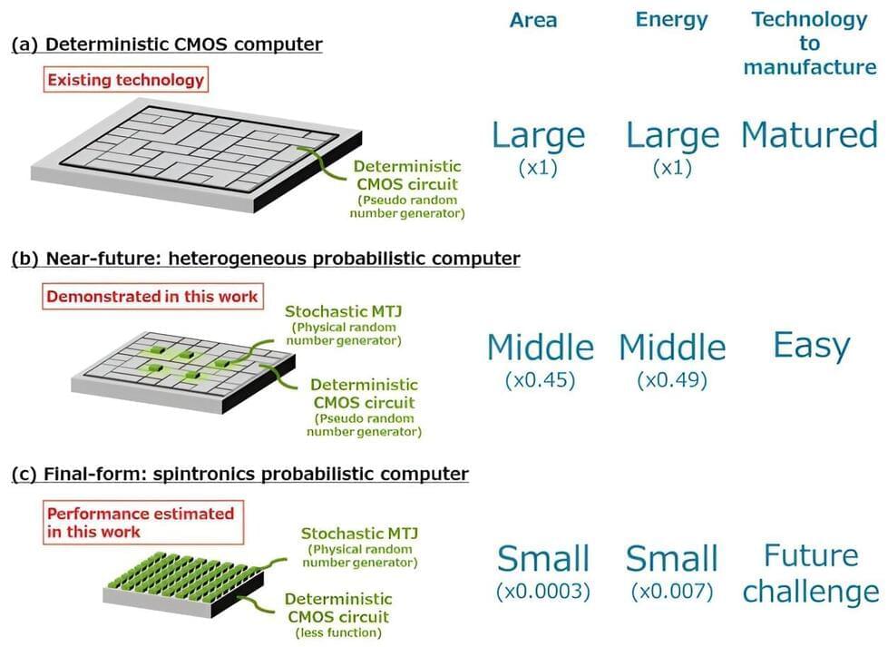
Toggle light / dark theme

From superfast magnetic levitation trains and computer chips to magnetic resonance imaging (MRI) machines and particle accelerators, superconductors are electrifying various aspects of our life. Superconductivity is an interesting property that allows materials to transfer moving charges without any resistance, below a certain critical point. This implies that superconducting materials can transfer electrical energy in a highly efficient manner without loss in the form of heat, unlike many conventional conductors.

Almost two decades ago scientists discovered superconductivity in a —magnesium diboride, or MgB2. There has been a resurgence in the of popularity MgB2 due to its low cost, superior superconducting abilities, high critical current density (which means that compared to other materials, MgB2 remains a semiconductor even when larger amounts of electric current is passed through it), and trapped magnetic fields arising from strong pinning of the vortices—which are cylindrical current loops or tubes of magnetic flux that penetrate a superconductor.

The intermetallic MgB2 also allows adjustability of its properties. For instance, the critical current density values (Jc) of MgB2 can be improved by decreasing the grain size and increasing the number of grain boundaries. Such adjustability is not observed in conventional layered superconductors.

“It’s akin to cutting holes or carving gullies in a super thin sheet of diamond, to ensure light travels and bounces in the desired direction,” he said.

To overcome the “etching” challenge, the researchers developed a new hard masking method, which uses a thin metallic tungsten layer to pattern the diamond nanostructure, enabling the creation of one-dimensional photonic crystal cavities.

Experimental video mashup on the Singularity featuring Ben Goertzel & Hugo de Garis.
Music by Scott Hanson (Tycho) — the actual song is Melanine form the album Dive.

Hugo de Garis
Ben Goertzel

Artilects
Nanotechnology

“I live on Earth at present, and I don’t know what I am. I know that I am not a category. I am not a thing — a noun. I seem to be a verb, an evolutionary process — an integral function of the universe.” — R. Buckminster Fuller I Seem to Be a Verb (1970)

Circa 2015 face_with_colon_three


From driving water wheels to turning turbines, waterhas been used as the prime mover of machinery and the powerhouse of industry for many centuries. In ancient times, the forces of flowing water were even harnessed to power the first rudimentaryclocks. Now, engineers at Stanford University have created the world’s first water-operated computer. Using magnetized particles flowing through a micro-miniature network ofchannels, the machine runs like clockwork and is claimed to be capable ofperforming complex logical operations.

Using poppy-seed sizeddroplets of water impregnated with magnetic nanoparticles (those handy little elementsbeing used in everything from drug delivery inhumans to creating e-paper whiteboards), the new fluidic computer uses electromagnetic fields to accurately pump thesedroplets around a set of physical gates to perform logical operations. Suspendedin oil and timed to move in very specific steps, the droplets in the system cantheoretically be used to accomplish any process that a normal electroniccomputer can, albeit at considerably slower speeds.

Circa 2014 face_with_colon_three


A liquid hard drive containing a suspension of nanoparticles could be used to store impressive amounts of data: 1 terabyte per tablespoon.

Researchers from the University of Michigan and New York University have been simulating wet information storage techniques which uses clusters of nanoparticles suspended in liquid. These clusters of particles can store more data than conventional computer bits which have just two storage states: 0 and 1. The clusters of particles work a bit like Rubik’s Cubes to reconfigure in different ways to represent different storage states. A 12-particle memory cluster connected to a central sphere can have almost eight million unique states, which is equivalent to 2.86 bytes of data.

The system works by having nanoparticles attached to a central sphere. When the sphere is small, the outer particles trap each other into place, storing data. If the sphere is a bit larger, the particles can be reconfigured to store different information. The team created a cluster involving four particles on a central sphere — all made of polymers. By heating the liquid up, the spheres expand and the particles can rearrange themselves in predictable ways. Although the four-particle clusters have only two distinguishable configurations (i.e. like a regular bit), the plan is create clusters with many more particles.

Researchers have reported a nano-sized neuromorphic memory device that emulates neurons and synapses simultaneously in a unit cell, another step toward completing the goal of neuromorphic computing designed to rigorously mimic the human brain with semiconductor devices.

Neuromorphic computing aims to realize (AI) by mimicking the mechanisms of neurons and that make up the . Inspired by the cognitive functions of the human brain that current computers cannot provide, neuromorphic devices have been widely investigated. However, current Complementary Metal-Oxide Semiconductor (CMOS)-based neuromorphic circuits simply connect artificial neurons and synapses without synergistic interactions, and the concomitant implementation of neurons and synapses still remains a challenge. To address these issues, a research team led by Professor Keon Jae Lee from the Department of Materials Science and Engineering implemented the biological working mechanisms of humans by introducing the neuron-synapse interactions in a single memory cell, rather than the conventional approach of electrically connecting artificial neuronal and synaptic devices.

Similar to commercial graphics cards, the artificial synaptic devices previously studied often used to accelerate parallel computations, which shows clear differences from the operational mechanisms of the human brain. The research team implemented the synergistic interactions between neurons and synapses in the neuromorphic memory device, emulating the mechanisms of the biological neural network. In addition, the developed neuromorphic device can replace complex CMOS neuron circuits with a single device, providing high scalability and cost efficiency.

After a 10-year research study that started by accident and was met with skepticism, a team of Northeastern University mechanical engineers was able to synthesize highly dense, ultra-narrow silicon nanowires that could revolutionize the semiconductor industry. Their research appears in Nature Communications.

Yung Joon Jung, Northeastern professor of mechanical and industrial engineering, says it might have been his favorite research project.

“Everything is new, and it required a lot of perseverance,” says Jung, who specializes in engineering and application of nanostructure systems and previously studied carbon nanotubes.

Accurate detection and manipulation of endogenous proteins is essential to understand cell biological processes, which motivated laboratories across cell biology to develop highly efficient CRISPR genome editing methods for endogenous epitope tagging (Auer et al., 2014; Nakade et al., 2014; Lackner et al., 2015; Schmid-Burgk et al., 2016; Suzuki et al., 2016; Nishiyama et al., 2017; Artegiani et al., 2020; Danner et al., 2021). Multiplex editing using NHEJ-based CRISPR/Cas9 methods remains limited because of the high degree of cross talk that occurs between two knock-in loci (Gao et al., 2019; Willems et al., 2020). In the current study we present CAKE, a mechanism to diminish cross talk between NHEJ-based CRISPR/Cas9 knock-ins using sequential activation of gRNA expression. We demonstrate that this mechanism strongly reduces cross talk between knock-in loci, and results in dual knock-ins for a wide variety of genes. Finally, we showed that CAKE can be directly applied to reveal new biological insights. CAKE allowed us to perform two-color super-resolution microscopy and acute manipulation of the dynamics of endogenous proteins in neurons, together revealing new insights in the nanoscale organization of synaptic proteins.

The CAKE mechanism presented here creates a mosaic of CreON and CreOFF knock-ins, and the number of double knock-in cells depends on the efficacy of each knock-in vector. Therefore, to obtain a high number of double knock-in cells, the efficacy of both the CreON and CreOFF knock-in vector must be optimized. We identified three parameters that regulate the efficacy for single and double knock-ins in neurons. First, the efficacy of gRNAs varies widely, and even gRNAs that target sequences a few base pairs apart in the same locus can have dramatically different knock-in rates (Willems et al., 2020; Danner et al., 2021; Fang et al., 2021; Zhong et al., 2021). Thus, the efficacy of each individual gRNA must be optimized to increase the chance of successful multiplex labeling in neurons. gRNA performance is dependent on many factors, including the rate of DNA cleavage and repair (Rose et al., 2017; Liu et al., 2020; Park et al.

Carnegie Mellon University researchers have pioneered the CMU Array—a new type of microelectrode array for brain computer interface platforms. It holds the potential to transform how doctors are able to treat neurological disorders.

The ultra-high-density microelectrode (MEA), which is 3D-printed at the nanoscale, is fully customizable. This means that one day, patients suffering from epilepsy or limb function loss due to stroke could have personalized medical treatment optimized for their individual needs.

The collaboration combines the expertise of Rahul Panat, associate professor of mechanical engineering, and Eric Yttri, assistant professor of biological sciences. The team applied the newest microfabrication technique, Aerosol Jet 3D printing, to produce arrays that solved the major design barriers of other brain computer interface (BCI) arrays. The findings were published in Science Advances.

Additive manufacturing techniques used to produce metal alloys have gained popularity due to their ability to be fabricated in complex shapes for use in various engineering applications. Yet the majority of studies conducted have centered around developing single-phase materials.

Dr. Kelvin Xie’s team in the Department of Materials Science and Engineering at Texas A&M University employed advanced characterization techniques to reveal the microstructure of the 3D-printed dual-phase multi-principal elements, also known as (HEAs), that display ultra-strong and ductile properties. This work is a collaboration with Dr. Wen Chen from the University of Massachusetts at Amherst and Dr. Ting Zhu from the Georgia Institute of Technology.

This study was recently published in Nature.