Toggle light / dark theme

Nanoengineers at the University of California San Diego have developed a new and potentially more effective way to deliver messenger RNA (mRNA) into cells. Their approach involves packing mRNA inside nanoparticles that mimic the flu virus—a naturally efficient vehicle for delivering genetic material such as RNA inside cells.

The new mRNA nanoparticles are described in a paper published recently in the journal Angewandte Chemie International Edition.

The work addresses a major challenge in the field of drug delivery: Getting large biological drug molecules safely into and protecting them from organelles called endosomes. These tiny acid-filled bubbles inside the cell serve as barriers that trap and digest large molecules that try to enter. In order for biological therapeutics to do their job once they are inside the cell, they need a way to escape the endosomes.

Skyrmions are ultra-stable atomic objects first discovered in real materials in 2009, which have more recently also been found also to exist at room temperatures. These unique objects have a number of desirable properties, including a substantially small threshold voltage, nanoscale sizes and easy electrical manipulation.

While these properties could be advantageous for the creation of a wide range of electronics, developing functional all– using skyrmions has so far proved to be very challenging. One possible application for skyrmions is in neuromorphic computing, which entails the creation of artificial structures that resemble those observed in the human brain.

With this in mind, researchers at the Korea Institute of Science and Technology (KIST) have recently investigated the possibility of using skyrmions to replicate mechanisms observed in the human brain. Their paper, published in Nature Electronics, shows that these ultra-stable atomic structures can be used to mimic some behaviors of biological synapses, which are junctions between neurons through which nerve impulses are passed on to different parts of the human brain.

A team of researchers from Nanjing University of Posts and Telecommunications and the Chinese Academy of Sciences in China and Nanyang Technological University and the Agency for Science Technology and Research in Singapore developed an artificial neuron that is able to communicate using the neurotransmitter dopamine. They published their creation and expected uses for it in the journal Nature Electronics.

As the researchers note, most machine-brain interfaces rely on as a communications medium, and those signals are generally one-way. Electrical signals generated by the brain are read and interpreted; signals are not sent to the brain. In this new effort, the researchers have taken a step toward making a that can communicate in both directions, and it is not based on electrical signals. Instead, it is chemically mediated.

The work involved building an artificial neuron that could both detect the presence of dopamine and also produce dopamine as a response mechanism. The neuron is made of graphene (a single sheet of carbon atoms) and a carbon nanotube electrode (a single sheet of carbon atoms rolled up into a tube). They then added a sensor capable of detecting the presence of dopamine and a device called a memristor that is capable of releasing dopamine using a heat-activated hydrogel, attached to another part of their artificial neuron.

Silicon is the second most abundant element on earth, making up a hefty 27.7% percent of the earth’s crust. Apart from its ability to create sandy beaches and clear glasses, silicon also holds the potential to make highly efficient metal ion batteries.

In a world where alternative energy storage devices like are gaining momentum, there is a need to harness the excellent specific energy capacity of silicon as an electrode material. The commercial application of silicon-based is often hindered due to two major reasons: 1) lack of mechanical stability arising from uncontrolled volume expansion upon lithiation, the process of combining with a , and 2) rapid energy fading caused by the formation of unstable solid-electrode interface (SEI) formation.

Over the years scientists have developed various advanced silicon-based negative electrodes or to overcome the aforementioned problems. The most prominent among them are silicon nanomaterials. However, silicon nanomaterials come with certain demerits, such as a large demand and supply gap, difficult and expensive synthesis process, and, most importantly, a threat of fast battery dry-up.

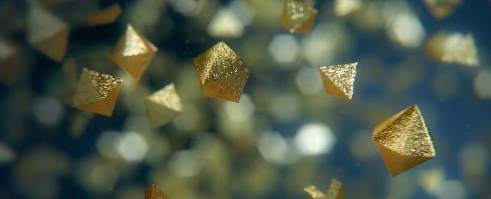
One convenient way to manipulate nanoscale objects with remote controllability is actuation and propulsion by light, which is largely based on optical and photothermal-induced forces. Unfortunately, the output of optical and photothermal-induced forces is small and speed is slow. This changes with a novel and intriguing nanoactuation system: plasmonic nanodynamite. This system can be optically triggered to eject gold nanobullets with an initial speed of up to 300 m/s.

Motors are ubiquitous in our everyday lives — from cars to washing machines, even if we rarely notice them. A futuristic scientific field is working on the development tiny motors that could power a network of nanomachines and replace some of the power sources we currently use in electronic devices.

Researchers from the Cockrell School of Engineering at The University of Texas at Austin created the first ever solid-state optical nanomotor. All previous iterations of these light-driven motors reside in a solution of some sort, which limited their potential for the majority of real-world applications. This new research was published recently in the journal ACS Nano.

“Life started in the water and eventually moved on land,” said Yuebing Zheng, an associate professor in the Walker Department of Mechanical Engineering. “We’ve made these micro nanomotors that have always lived in solution work on land, in a solid state.”

Helium ion beam (HIB) technology plays an important role in the extreme fields of nanofabrication. Due to high resolution and sensitivity, HIB nanofabrication technology is widely used to pattern nanostructures into components, devices, or systems in integrated circuits, materials sciences, nano-optics, and bio-sciences applications. HIB-based nanofabrication includes direct-write milling, ion beam-induced deposition, and direct-write lithography without the need to resist assistance. Their nanoscale applications have also been evaluated in the areas of integrated circuits, materials sciences, nano-optics, and biological sciences.

In a new paper published in the International Journal of Extreme Manufacturing, a team of researchers, led by Dr. Deqiang Wang from Chongqing Key Laboratory of Multi-scale Manufacturing Technology, Chongqing Institute of Green and Intelligent Technology, Chinese Academy of Sciences, PR China, have summarized comprehensively the extreme processes and applications of HIB .

The main aim of this review is to address the latest developments in HIB with their extreme processing capabilities and widespread applications in nanofabrication. Based on the introduction of the HIM system with GFIS, the performance characteristics and advantages of HIB technology have been discussed first. Thereafter, certain questions about the extreme processes and applications of HIB nanofabrication have been addressed: How many extreme processes and applications of HIB technology have been developed in nanofabrication for integrated circuits, materials sciences, nano-optics, and bio-sciences applications? What are the main challenges in the extreme nanofabrication with HIB technology for high resolution and sensitivity applications?

3D micro-/nanofabrication holds the key to building a large variety of micro-/nanoscale materials, structures, devices, and systems with unique properties that do not manifest in their 2-D planar counterparts. Recently, scientists have explored some very different 3D fabrication strategies such as kirigami and origami that make use of the science of cutting and folding 2-D materials/structures to create versatile 3D shapes. Such new methodologies enable continuous and direct 2-D-to-3D transformations through folding, bending and twisting, with which the occupied space can vary “nonlinearly” by several orders of magnitude compared to the conventional 3D fabrications. More importantly, these new-concept kirigami/origami techniques provide an extra degree of freedom in creating unprecedented 3D micro-/nanogeometries beyond the imaginable designs of conventional subtractive and additive fabrication.

In a new paper published in Light: Science & Applications, Chinese scientists from Beijing Institute of Technology and South China University of Technology made a comprehensive review on some of the latest progress in kirigami/origami in micro-/nanoscale. Aiming to unfold this new regime of advanced 3D micro-/nanofabrication, they introduced and discussed various stimuli of kirigami/origami, including capillary force, residual stress, mechanical stress, responsive force and focused-ion-beam irradiation induced stress, and their working principles in the micro-/nanoscale region. The focused-ion-beam based nano-kirigami, as a prominent example coined in 2018 by the team, was highlighted particularly as an instant and direct 2-D-to-3D transformation technique. In this method, the focused ion beam was employed to cut the 2-D nanopatterns like “knives/scissors” and gradually “pull” the nanopatterns into complex 3D shapes like “hands”.