Menu

Blog

Archive for the ‘materials’ category: Page 98

Jun 18, 2022

Scientists serendipitously discover rare cluster compound

Posted by in categories: biotech/medical, materials

Scientists at Kyoto University’s Institute for Cell-Material Sciences have discovered a novel cluster compound that could prove useful as a catalyst. Compounds, called polyoxometalates, that contain a large metal-oxide cluster carry a negative charge. They are found everywhere, from anti-viral medicines to rechargeable batteries and flash memory devices.

The new cluster compound is a hydroxy-iodide (HSbOI) and is unusual, as it has large, positively charged clusters. Only a handful of such positively charged cluster compounds have been found and studied.

“In , the discovery of or molecule can create a new science,” says Kyoto University chemist Hiroshi Kageyama. “I believe that these new positively charged clusters have great potential.”

Jun 17, 2022

Did supernovae help form Barnard’s Loop?

Posted by in categories: cosmology, materials

Astronomers studying the structure of the Milky Way galaxy have released the highest-resolution 3D view of the Orion star-forming region. The image and interactive figure were presented today at a press conference hosted by the American Astronomical Society.

Led by researchers at the Center for Astrophysics | Harvard & Smithsonian, the work connects 3D data on young stars and interstellar gas around the Orion complex of star-forming regions. Analysis of the 2D and 3D images, alongside theoretical modeling, shows that supernova explosions within the last 4 million years produced large cavities in the interstellar material associated with Orion.

Continue reading “Did supernovae help form Barnard’s Loop?” »

Jun 16, 2022

Automating semiconductor research with machine learning

Posted by in categories: materials, robotics/AI

The semiconductor industry has been growing steadily ever since its first steps in the mid-twentieth century and, thanks to the high-speed information and communication technologies it enabled, it has given way to the rapid digitalization of society. Today, in line with a tight global energy demand, there is a growing need for faster, more integrated, and more energy-efficient semiconductor devices.

However, modern semiconductor processes have already reached the nanometer scale, and the design of novel high-performance materials now involves the structural analysis of semiconductor nanofilms. Reflection high-energy electron diffraction (RHEED) is a widely used analytical method for this purpose. RHEED can be used to determine the structures that form on the surface of thin films at the atomic level and can even capture structural changes in real time as the thin film is being synthesized!

Unfortunately, for all its benefits, RHEED is sometimes hindered by the fact that its output patterns are complex and difficult to interpret. In virtually all cases, a highly skilled experimenter is needed to make sense of the huge amounts of data that RHEED can produce in the form of diffraction patterns. But what if we could make machine learning do most of the work when processing RHEED data?

Jun 15, 2022

New member added to carbon material family, a two-dimensional monolayer polymeric fullerene

Posted by in category: materials

Synthetic carbon allotropes are fascinating for their outstanding properties and potential applications. Scientists have devoted decades to synthesizing new types of carbon materials. However, a two-dimensional fullerene, which possesses a unique structure, has not been successfully synthesized until now.

A research group led by Prof. Zheng Jian from the Institute of Chemistry of the Chinese Academy of Sciences (ICCAS) developed a new interlayer bonding cleavage strategy to prepare a two-dimensional polymeric fullerene.

The researchers prepared magnesium intercalated C60 bulk crystals as the precursor to the exfoliation reaction. They then utilized a ligand-assisted cation exchange strategy to cleave the interlayer bonds into bulk crystals, which led to the bulk crystals being exfoliated into monolayer nanosheets.

Jun 13, 2022

Researchers solve mystery surrounding dielectric properties of unique metal oxide

Posted by in categories: computing, materials

A University of Minnesota Twin Cities-led research team has solved a longstanding mystery surrounding strontium titanate, an unusual metal oxide that can be an insulator, a semiconductor, or a metal. The research provides insight for future applications of this material to electronic devices and data storage.

The paper is published in the Proceedings of the National Academy of Sciences.

When an insulator like is placed between oppositely charged , the electric field between the plates causes the negatively charged electrons and the positive nuclei to line up in the direction of the field. This orderly lining up of electrons and nuclei is resisted by thermal vibrations, and the degree of order is measured by a fundamental quantity called the . At low temperature, where the thermal vibrations are weak, the dielectric constant is larger.

Jun 12, 2022

These NanoLeaf-Inspired Modular Lights Can Team Up to Create a Wall-Mounted Four-Digit Display

Posted by in categories: materials, space

Built using a 3D-printed framework and an Espressif ESP32, this modular lighting system can double as a display.


Hoag’s Object is a galaxy with an central region and a bright outer ring, but lacks any intervening material.

Continue reading “These NanoLeaf-Inspired Modular Lights Can Team Up to Create a Wall-Mounted Four-Digit Display” »

Jun 12, 2022

Weird Object: Hoag’s Object

Posted by in categories: materials, space

Hoag’s Object is a galaxy with an central region and a bright outer ring, but lacks any intervening material.


No. 7: With This Ring, I Thee Puzzle.

In 1950, astronomer Arthur Hoag came upon a tiny, faint, 16th-magnitude ring surrounding a ball-like center, and reasonably assumed it was a planetary nebula — a nearby puff of gas expelled from a single old-aged star. He also proposed an alternative and far more exotic explanation that this was an “Einstein Ring” from a faraway quasar. In this scenario, the quasar’s light is distorted into a halo by space-warping caused by a massive foreground spherical galaxy that it seems to surround. But later spectroscopic studies rejected this because the golden central ball and the blue ring have exactly the same redshift, indicating a whopping rush-away speed of 7,916 miles (12,740 kilometers) per second, which proves they’re both located exactly the same distance from us.

Jun 12, 2022

Back: This is a video so many of you have asked for!

Posted by in category: materials

In this material, you will find strange objects, phenomena, and formations on the red planet. Some of them are explained and others remain mysterious to this day.

Jun 12, 2022

AI solution makes the quest for elusive monolayers a lot simpler

Posted by in categories: materials, robotics/AI

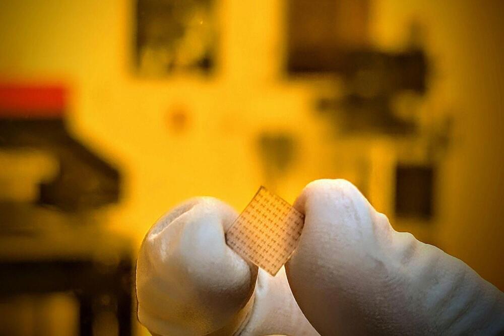
One of the most tedious, daunting tasks for undergraduate assistants in university research labs involves looking hours on end through a microscope at samples of material, trying to find monolayers.

These —less than 1/100,000th the width of a human hair—are highly sought for use in electronics, photonics, and because of their unique properties.

“Research labs hire armies of undergraduates to do nothing but look for monolayers,” says Jaime Cardenas, an assistant professor of optics at the University of Rochester. “It’s very tedious, and if you get tired, you might miss some of the monolayers or you might start making misidentifications.”

Jun 10, 2022

Graphene charge-injection photodetectors with a broader detection bandwidth

Posted by in categories: materials, particle physics

Photodetectors, sensors that can detect light or other forms of electromagnetic radiation, are essential components of imaging tools, communication systems, and various other technologies on the market. These sensors work by converting photons (i.e., light particles) into electrical current.

Researchers at Zhejiang University have recently developed a new photodetector that could detect light within a broader bandwidth. Their device, presented in a paper published in Nature Electronics, could be used to develop new and more advanced imaging technologies.

“Our recent project is based on traditional charge-coupled device (CCD) and complementary metal-oxide-semiconductor (CMOS) imaging technologies,” Prof. Yang Xu, one of the researchers who carried out the study, told TechXplore. “Our novel imaging devices combining CCD’s MOS photogate for and CMOS’s independent pixel structure can significantly benefit monolithic integration, performance, and readout.”