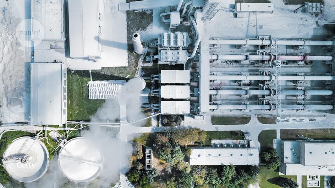
Concrete will be crucial for much-needed climate-resilient construction. But the cement industry must set out its plan for decarbonization.
Researchers from Kyoto University have achieved a significant advancement in materials science by developing the world’s first three-dimensional van der Waals open frameworks (WaaFs). This innovation challenges the conventional belief that van der Waals interactions are too weak for open framework materials, demonstrating their potential for stable and highly porous materials.
Published in Nature Chemistry, the study presents a strategy using octahedral metal-organic polyhedra (MOPs) as building blocks to construct WaaFs. These frameworks exhibit high thermal stability, exceptional porosity, and reversible assembly, opening new avenues for applications in gas storage, separation, and catalysis.
WaaFs utilize van der Waals interactions, which were previously considered too weak, to form robust three-dimensional frameworks. These structures maintain their integrity at temperatures up to 593 K and achieve surface areas exceeding 2,000 m2/g, making them highly stable and efficient for various industrial applications.
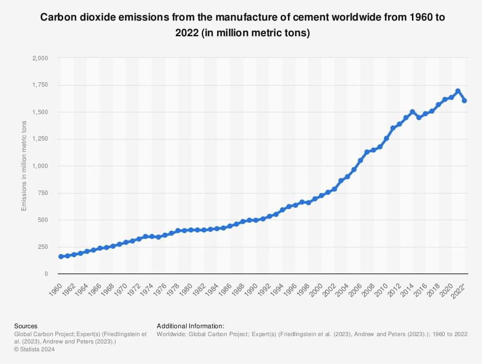
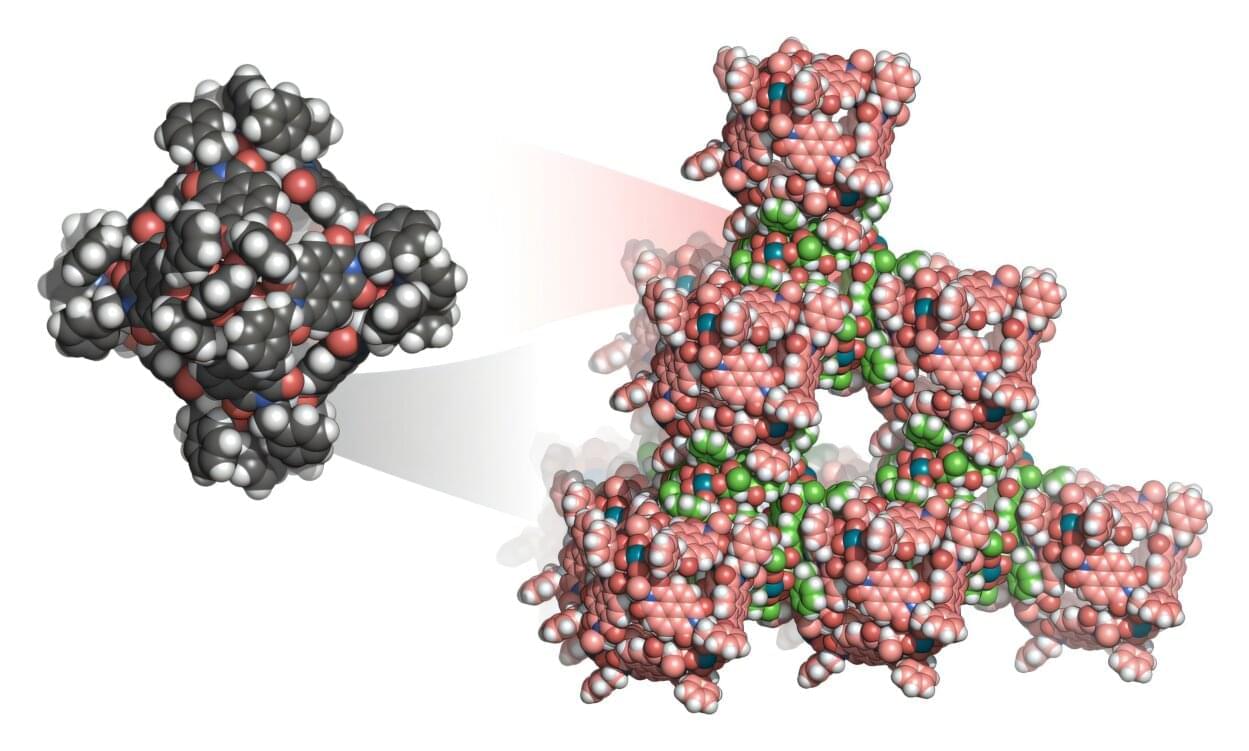
Researchers at the University of Liverpool and the University of Southampton have used computational design methods to develop non-metal organic porous framework materials, with potential applications in areas such as catalysis, water capture or hydrogen storage.
In a study published in the journal Nature, the research team used inexpensive and abundant non-metallic elements, such as chloride ions, to design non-metal organic porous frameworks (N-MOFs).
The new materials offer an alternative to metal-organic frameworks (MOFs), a class of porous, crystalline materials made up of metals connected by organic linker compounds.
The Burj Khalifa, the tallest building in the world, employs advanced construction techniques designed to withstand wind, seismic activity, and its own massive weight. Among these techniques is the “Meta Column System,” which plays a pivotal role by strategically positioning large columns to resist lateral forces, thereby facilitating the construction of such a towering structure.
What if these advanced architectural techniques could be applied to material design?
Metal-Organic Frameworks (MOFs) are porous materials formed by the combination of metal ions and organic ligands, resulting in structures similar to rebar in buildings. The design principle underlying MOFs closely resembles architectural planning.
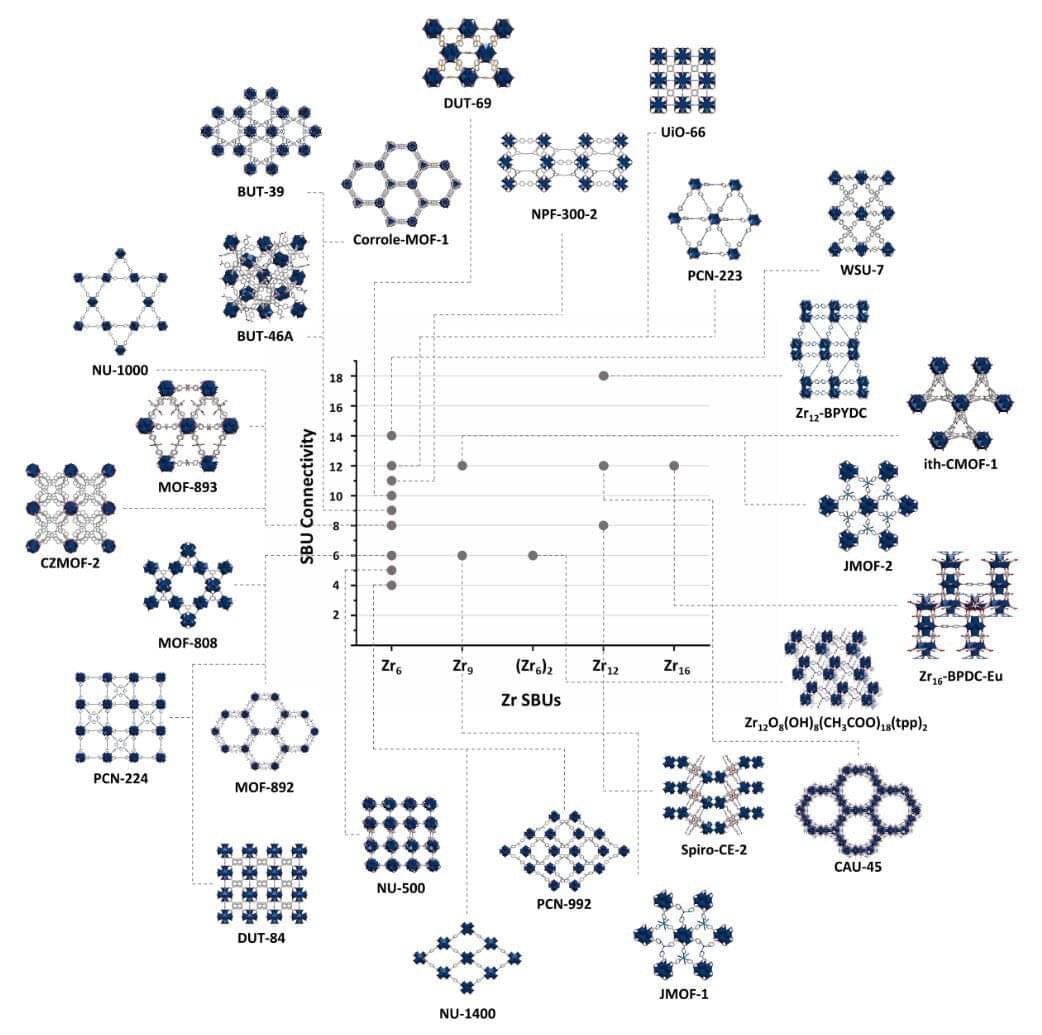
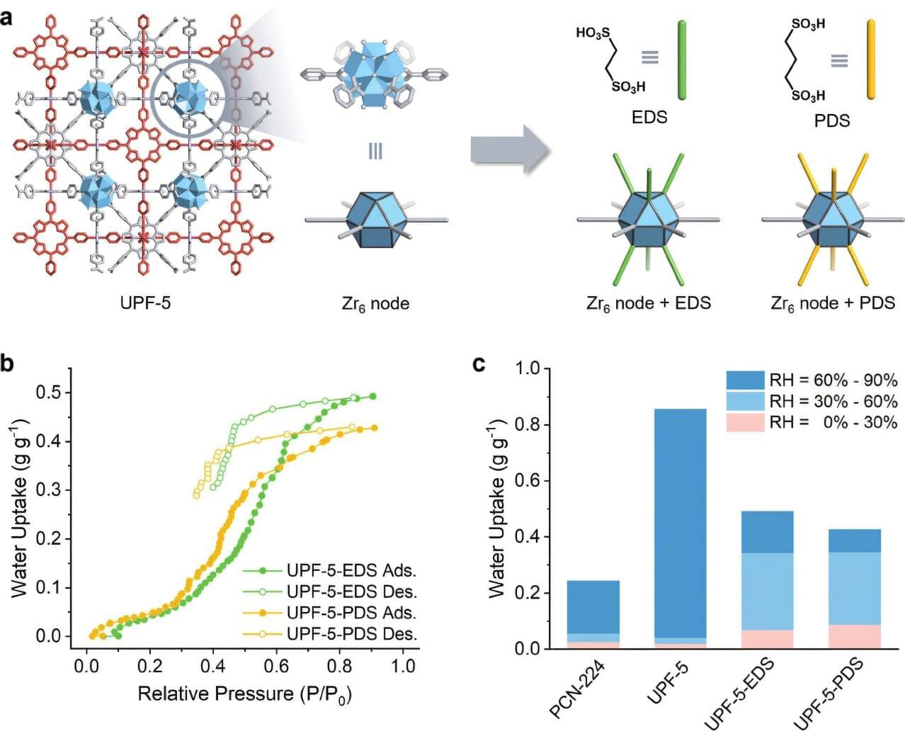
Metal-organic frameworks (MOFs) have been gaining attention as promising carbon-neutral porous materials, thanks to their high performance in gas storage, separation, and conversion. The geometric building blocks of MOFs, metal clusters and organic linkers, allow chemists to predict and synthesize new structures like assembling LEGO. However, finding new metal building blocks is still a daunting challenge due to the complex nature of metal ions in synthesis.
A research team, led by Professor Wonyoung Choe at Ulsan National Institute of Science and Technology (UNIST), South Korea, was inspired by the molecular metal clusters previously synthesized before realized in porous materials. This implies one can predict future MOFs by looking closely at their metal building blocks.
The research team compared zirconium metal clusters found in both MOFs and molecules. Zirconium-based MOFs are one of the representative metal-organic porous materials with remarkable stability and a broad range of applications. The researchers identified seven types of zirconium building blocks in MOFs and discovered additional fourteen types of potential metal building blocks.
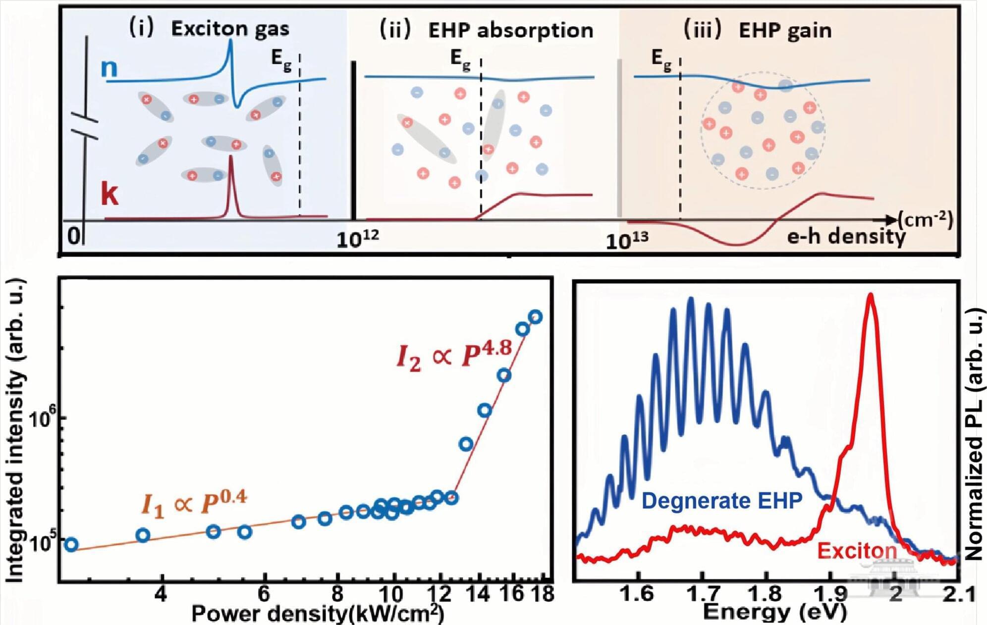
Amplified spontaneous emission is a physical phenomenon that entails the amplification of the light spontaneously emitted by excited particles, due to photons of the same frequency triggering further emissions. This phenomenon is central to the functioning of various optoelectronic technologies, including lasers and optical amplifiers (i.e., devices designed to boost the intensity of light).
The excitation of a material with high-energy photons can produce what is known as an electron-hole plasma. This state is characterized by the dense presence of negatively charged particles (i.e., electrons) and positively charged vacancies (i.e., holes).
Researchers at Wuhan University recently observed amplified spontaneous emission originating from degenerate electron-hole plasma in a 2D semiconductor, namely suspended bilayer tungsten disulfide (WS2). Their paper, published in Physical Review Letters, could pave the way for the development of new optoelectronic technologies based on 2D semiconductors.
Researchers have uncovered a surprising phenomenon in the material BiNiO3: when subjected to high pressure at low temperatures, its well-arranged electrical charges are disrupted, leading to a disordered “charge glass” state.
The study is published in the journal Nature Communications.
This discovery offers new insights into how materials respond to extreme conditions, potentially paving the way for new advanced materials with unique and useful properties.
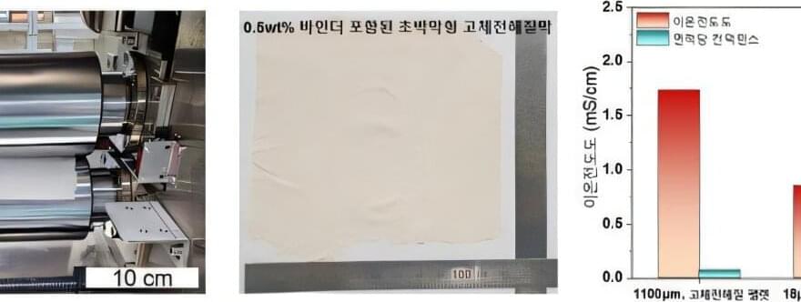
Korean researchers have succeeded in developing a key technology for all-solid-state secondary batteries, known as next-generation lithium-ion batteries due to their high safety. The work was published online as a cover study in Small at the end of last year.
Electronics and Telecommunications Research Institute (ETRI) developed a separation membrane based on a binder material that easily becomes fibrillized when subjected to mechanical shearing (force applied) through a mixing process with solid electrolyte powder without using a solvent. This solid electrolyte membrane is simple and fast to manufacture and is extremely thin and robust.
In general, in research on all-solid-state secondary batteries, the thickness is set to several hundred micrometers (µm) to 1 millimeter (mm) to increase the durability of the membrane when using a hard solid electrolyte in the manufacturing process. However, this has the disadvantage of being too thick compared to conventional polymer separation membranes, resulting in a very large loss of energy density.
