Magnets and superconductors go together like oil and water—or so scientists have thought. But a new finding by MIT physicists is challenging this century-old assumption.
In a paper appearing in the journal Nature, the physicists report that they have discovered a “chiral superconductor”—a material that conducts electricity without resistance, and also, paradoxically, is intrinsically magnetic. What’s more, they observed this exotic superconductivity in a surprisingly ordinary material: graphite, the primary material in pencil lead.
Graphite is made from many layers of graphene—atomically thin, lattice-like sheets of carbon atoms—that are stacked together and can easily flake off when pressure is applied, as when pressing down to write on a piece of paper. A single flake of graphite can contain several million sheets of graphene, which are normally stacked such that every other layer aligns. But every so often, graphite contains tiny pockets where graphene is stacked in a different pattern, resembling a staircase of offset layers.
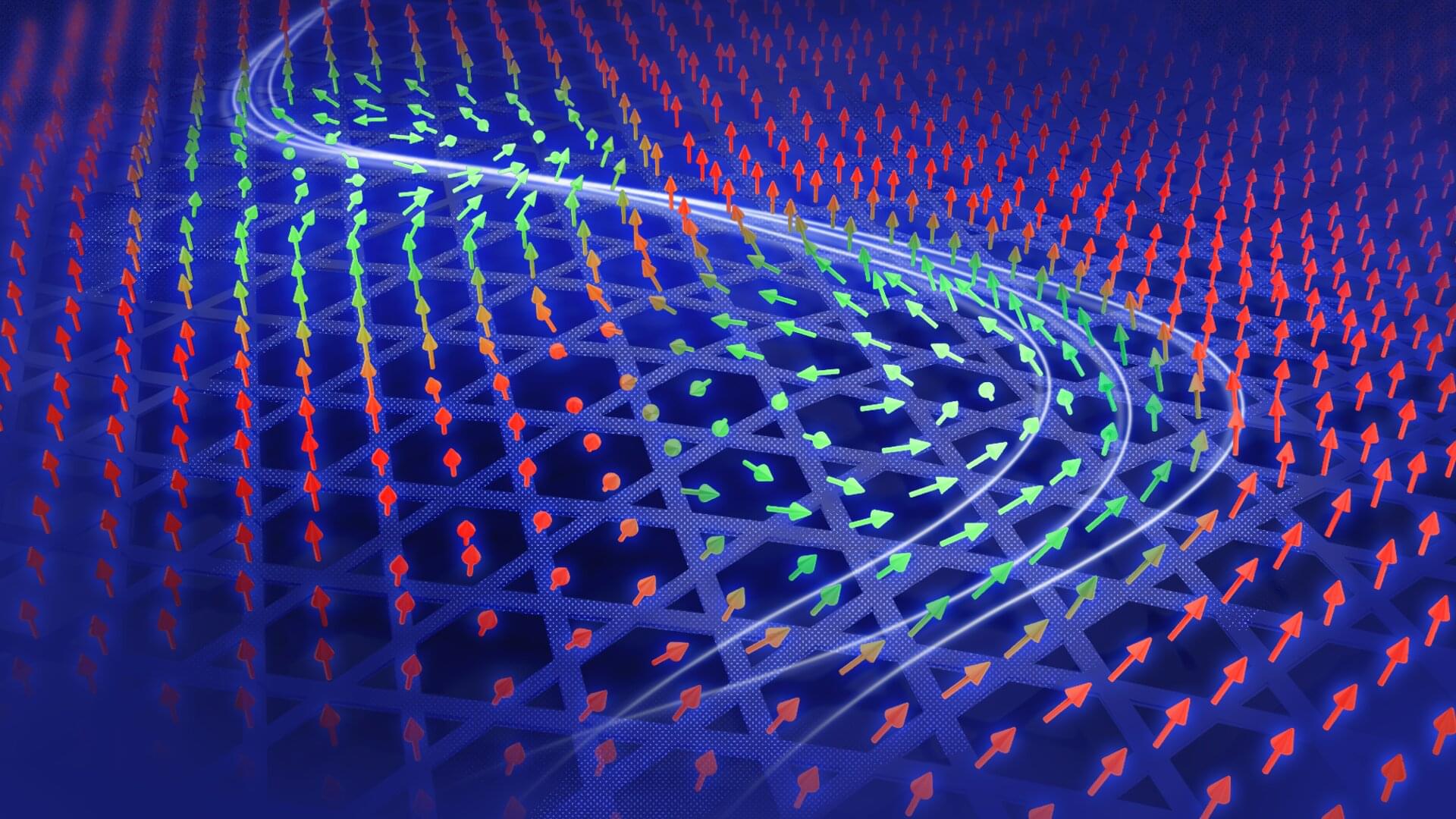

