The flexible lasers, less than a thousandth of a millimetre thick, work as free-standing films and can stick to different materials including banknotes and contact lenses.
https://www.gizmodo.com.au/…/science-has-peaked-we-can-now…/
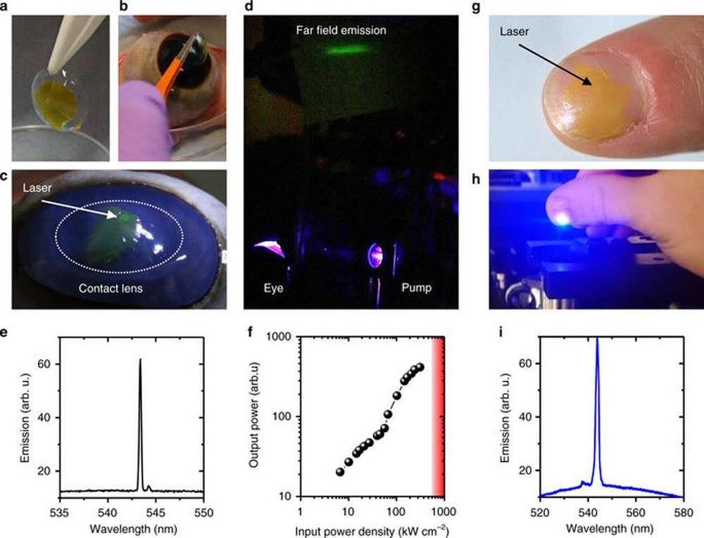
The flexible lasers, less than a thousandth of a millimetre thick, work as free-standing films and can stick to different materials including banknotes and contact lenses.
https://www.gizmodo.com.au/…/science-has-peaked-we-can-now…/

Dimensions: 3.5″ x 3.0″ x 1.8″ Date: 1993 Material: original stone is virginia albamarle serpentine, reproductions silicon bronze Special Engraving: the matrix (0,1 | 1,1) Weight: 4 oz Copyright Notice: © 1993 Copyright Registered: 1996.
The Fibonacci numbers are ubiquitious in nature and mathematics. This palmsize sculpture encapsulates the generating matrix for these numbers. In a problem published 800 years ago, Leonardo of Pisa, a.k.a. Fibonacci formulated his famous rabbit problem: beginning with a newborn fertile pair of rabbits, how many pairs will accumulate monthly if each pair produces another pair from their second month on? The solution of this leads to a recursively defined sequence of integers, 0, 1, 1, 2, 3, 5, 8, 13, 21, 34, 55, 89, 144, … This sequence has the property that two consequtive terms added give the next term.
The Fibonacci Matrix Torus has raised (esker) curves or continuous crests which wind around the torus either the short way or both the short and long way. This gives the matrix with first row (0, 1) and second row (1, 1) respectively. The powers of this matrix give matrices whose entries are always Fibonacci numbers.
A research group from RIKEN and Kyushu University has developed a new type of material, based on ethylene, which exhibits a number of useful properties such as self-healing and shape memory. Remarkably, some of the materials can spontaneously self-heal even in water or acidic and alkali solutions. The new material is based on ethylene, a compound that is the source of much of the plastic in use today.
Materials that can self-heal have become a popular area of research during the last decade, and a variety of materials have been developed. However, most of the self-healing materials reported to date have relied on sophisticated designs that incorporate chemical mechanisms into polymer networks, such as irreversible or reversible covalent-bond formation, hydrogen bonding, metal-ligand interactions, or ionic interactions. As a result, they require some external stimulus, such as heat or pressure, to prompt them to heal, and in most cases, they do not function in water, acid or alkaline solutions because the chemical networks cannot survive such conditions. The ideal is to create a material that possesses sufficient toughness and can autonomously self-heal under various conditions.
For the present research, published in the Journal of the American Chemical Society, the researchers used a catalyst based on scandium, a rare metal, to create polymers composed of alternating sequences of ethylene and anisylpropylenes and shorter ethylene-ethylene segments by the copolymerization of ethylene and anisylpropylenes. This new class of well-defined, functionalized polyolefins ranged from soft viscoelastic materials—materials that can be both elastic but also exhibit liquid-like properties—to tough elastomers, which can be stretched but return to their original shapes, and rigid plastics. The elastomer copolymers were very elastic, and tough, and also showed remarkable self-healing property, as they autonomously self-healed when subjected to mechanical damage not only in a dry environment but also in water and aqueous acid and alkaline solutions, without the need for any external energy or stimulus.
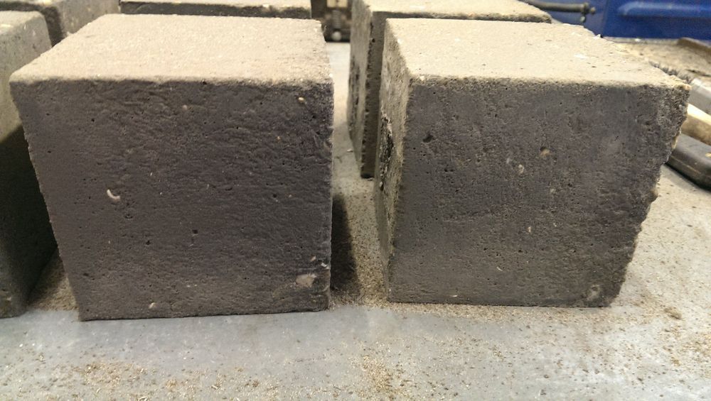
A new greener, stronger and more durable concrete that is made using the wonder-material graphene could revolutionise the construction industry.
Experts from the University of Exeter have developed a pioneering new technique that uses nanoengineering technology to incorporate graphene into traditional concrete production.
The new composite material, which is more than twice as strong and four times more water resistant than existing concretes, can be used directly by the construction industry on building sites. All of the concrete samples tested are according to British and European standards for construction.
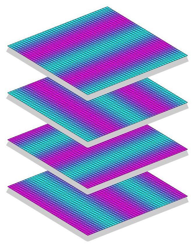
Scientists seeking to understand the mechanism underlying superconductivity in “stripe-ordered” cuprates—copper-oxide materials with alternating areas of electric charge and magnetism—discovered an unusual metallic state when attempting to turn superconductivity off. They found that under the conditions of their experiment, even after the material loses its ability to carry electrical current with no energy loss, it retains some conductivity—and possibly the electron (or hole) pairs required for its superconducting superpower.
“This work provides circumstantial evidence that the stripe-ordered arrangement of charges and magnetism is good for forming the charge-carrier pairs required for superconductivity to emerge,” said John Tranquada, a physicist at the U.S. Department of Energy’s Brookhaven National Laboratory.
Tranquada and his co-authors from Brookhaven Lab and the National High Magnetic Field Laboratory at Florida State University, where some of the work was done, describe their findings in a paper just published in Science Advances. A related paper in the Proceedings of the National Academy of Sciences by co-author Alexei Tsvelik, a theorist at Brookhaven Lab, provides insight into the theoretical underpinnings for the observations.
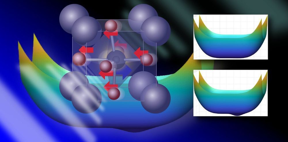
Most people think of water as existing in only one of three phases: Solid ice, liquid water, or gas vapor. But matter can exist in many different phases—ice, for example, has more than ten known phases, or ways that its atoms can be spatially arranged. The widespread use of piezoelectric materials, such as microphones and ultrasound, is possible thanks to a fundamental understanding of how an external force, like pressure, temperature, or electricity, can lead to phase transitions that imbue materials with new properties.

The gold vapor laser has been widely used in the treatment of cancer using photodynamic therapy.
Using Blue Light to See Through Fire in Optical Imaging Dr Matthew Hoehler AZoOptics talks to Dr Matthew Hoehler about his recent research, using blue light to see through fires and make previously impossible qualitative observations about material damage during a fire.
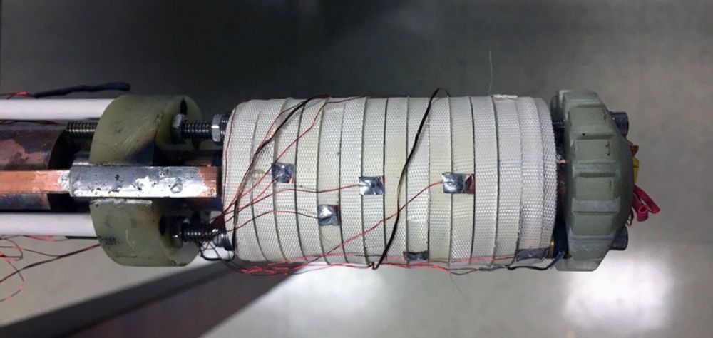
A new superconducting magnet has briefly sustained an astonishing 45.5 tesla magnetic field intensity. For comparison, your flimsy fridge magnets have about 1 percent of a single tesla.
The measurement, achieved by researchers at the National High Magnetic Field Laboratory (MagLab) at Florida State University resets the bar on what’s possible in direct current magnetic fields, exceeding the previous limit by half a tesla.
MagLab already houses the world’s strongest continuous magnet, a hybrid that relies on pairing an insanely cold superconductor with a more typical electromagnet to operate.

SpaceX’s next mission for its Falcon Heavy high-capacity rocket is set for June 24, when it’ll take off from NASA’s Kennedy Space Center in Florida with 20 satellites on board that comprise the Department of Defense’s Space Test Program-2. That’s not all it’ll carry however: There also will be cargo pertaining to four NASA missions aboard the private launch vehicle, including materials that will support the Deep Space Atomic Clock, the Green Propellant Infusion Mission and two payloads that will serve scientific missions.
NASA detailed all of these missions in a press conference today, going into more detail about what each will involve and why NASA is even pursuing this research to begin with.