Archive for the ‘materials’ category: Page 280
Jul 8, 2016
Tunable wetting and adhesion of graphene demonstrated
Posted by Karen Hurst in categories: engineering, materials
Nice.
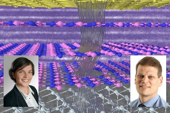
“Our study suggests for the first time that the doping-induced modulation of the charge carrier density in graphene influences its wettability and adhesion,” explained SungWoo Nam, an assistant professor in the Department of Mechanical Science and Engineering at Illinois. “This work investigates this new doping-induced tunable wetting phenomena which is unique to graphene and potentially other 2D materials in complementary theoretical and experimental investigations.”
Graphene, being optically transparent and possessing superior electrical and mechanical properties, can revolutionize the fields of surface coatings and electrowetting displays, according to the researchers. A material’s wettability (i.e. interaction with water) is typically constant in the absence of external influence and are classified as either water-loving (hydrophilic) or water-repelling (hydrophobic; water beads up on the surface). Depending on the specific application, a choice between either hydrophobic or hydrophilic material is required. For electrowetting displays, for example, the hydrophilic characteristics of display material is enhanced with the help of a constant externally impressed electric current.
Continue reading “Tunable wetting and adhesion of graphene demonstrated” »
Jul 6, 2016
Super-strong and airy 3D-printed supermaterials inch closer to reality
Posted by Karen Hurst in categories: 3D printing, materials
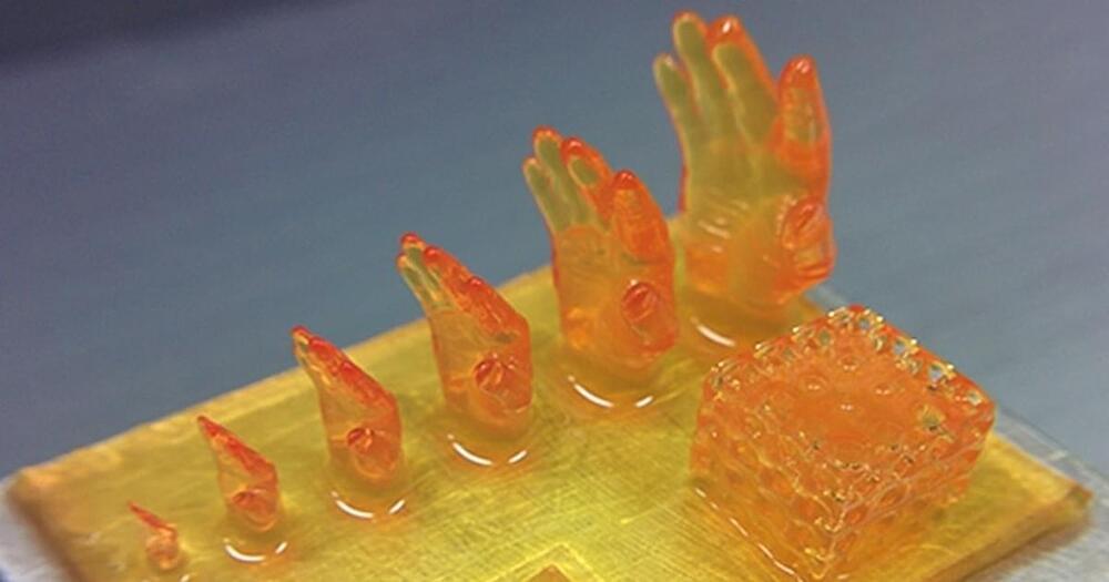
Researchers at the Masdar Institute are creating 3D printed high performance materials with custom-designed mechanical, thermal and electrical properties by manipulating the materials’ internal structures.
Jul 4, 2016
Injectable biomaterial could be used to manipulate organ behavior
Posted by Karen Hurst in categories: biotech/medical, materials
Way cool.
Ideally, injectable or implantable medical devices should not only be small and electrically functional, they should be soft, like the body tissues with which they interact. Scientists from two UChicago labs set out to see if they could design a material with all three of those properties.
The material they came up with, published online June 27, 2016, in Nature Materials, forms the basis of an ingenious light-activated injectable device that could eventually be used to stimulate nerve cells and manipulate the behavior of muscles and organs.
Continue reading “Injectable biomaterial could be used to manipulate organ behavior” »
Jul 2, 2016
New material switches from water-repelling to water-loving with electric current
Posted by Karen Hurst in categories: materials, nanotechnology
Definitely makes sense when you consider how things work in nature.
Generally, water repellent objects and those that attract or absorb water have very different microscopic-level attributes that endow them with their behavior. For example, the myriad tiny hairs on a gecko’s body help it to efficiently repel water, whilst specially treated cotton designed for harvesting water from the air contains millions of tiny pores that draw in liquid. Now researchers have discovered a way to use a single type of material to perform both functions, switching between liquid attraction and liquid repulsion, simply through the application of an electric voltage.
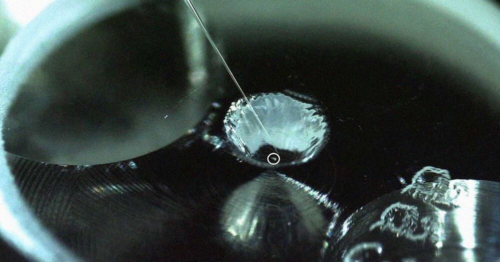
Developed by a team of scientists from TU Wien, the University of Zurich, and KU Levin, the new material alters its water-handling behavior by changing its surface structure at the nanoscale to effect a change at the macroscale. Specifically, the behavior of liquid on the new material is as a result of altering the “stiction” (static friction) of the molecular surface. One with a high-level of stiction keeps moisture clinging to it, whilst one with a low-level allows the liquid to run right off.
Jul 1, 2016
MIT graphene breakthrough could make chips one million times faster
Posted by Shailesh Prasad in categories: computing, materials
Researchers use graphene to create a new way of converting electricity into light, delivering the possibility of dramatic speed improvements over today’s chips.
Jun 17, 2016
Map of diamond-boron bond paves way for new materials
Posted by Karen Hurst in category: materials
Great writeup and goes well with the other posting on DiAmanti’s new perfected synthetic diamonds.
Scientists in Japan have successfully recorded the atomic bonds between diamond and cubic boron nitride: the hardest known materials on earth. This feat could ultimately lead to the design of new types of semiconductors.
Diamond is the hardest material in existence but is useless for cutting steel because it reacts with iron, from which steel is made, at high temperatures. Cubic boron nitride, a synthetic material, is the second hardest substance after diamond but is chemically stable against iron at high temperatures. If desirable composites of diamond and cubic boron nitride crystals could be obtained, a unique machining tool could be developed for work on hard rock and substances that contain iron. Also, a better understanding of the bonds formed between these two unique semiconducting materials could lead to the development of new types of semiconductors. The nature of these bonds was previously unknown.
Continue reading “Map of diamond-boron bond paves way for new materials” »
Jun 15, 2016
BioArtist Grows A Sculpture Out Of Bone
Posted by Shailesh Prasad in category: materials
Jun 15, 2016
Researchers discover new way to turn electricity into light, using graphene
Posted by Andreas Matt in category: materials
Researchers at MIT and elsewhere have found a new way of generating light and other electromagnetic radiation, using a sheet of graphene, a pure two-dimensional form of carbon.
Jun 14, 2016
X-ray Experiments Show Hewlett Packard Team How Memristors Work
Posted by Andreas Matt in categories: computing, materials
In experiments at two Department of Energy national labs – SLAC National Accelerator Laboratory and Lawrence Berkeley National Laboratory – scientists at Hewlett Packard Enterprise (HPE) have experimentally confirmed critical aspects of how a new type of microelectronic device, the memristor, works at an atomic scale.
This result is an important step in designing these solid-state devices for use in future computer memories that operate much faster, last longer and use less energy than today’s flash memory. The results were published in February in Advanced Materials.
“We need information like this to be able to design memristors that will succeed commercially,” said Suhas Kumar, an HPE scientist and first author on the group’s technical paper.
Continue reading “X-ray Experiments Show Hewlett Packard Team How Memristors Work” »