Toggle light / dark theme

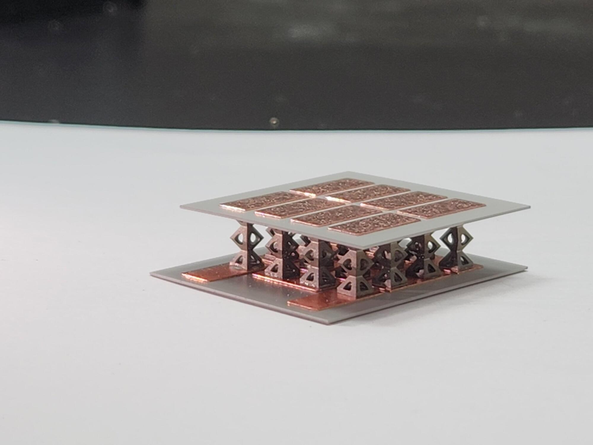
Researchers have succeeded in developing a framework for organic thermoelectric power generation from ambient temperature and without a temperature gradient. Thermoelectric devices are devices that can convert heat into electrical energy. Researchers have now developed a thermoelectric device composed of organic materials that can generate electricity from ambient temperature alone. The device is made from copper phthalocyanine and copper hexadecafluoro phthalocyanine as charge $transfer materials and was combined with fullerenes and BCP as electron transport layers.

Researchers have developed a new organic thermoelectric device that can harvest energy from ambient temperature. While thermoelectric devices have several uses today, hurdles still exist to their full utilization. By combining the unique abilities of organic materials, the team succeeded in developing a framework for thermoelectric power generation at room temperature without any temperature gradient. Their findings were published in the journal Nature Communications.

Thermoelectric devices, or thermoelectric generators, are a series of energy-generating materials that can convert heat into electricity so long as there is a temperature gradient — where one side of the device is hot and the other side is cool. Such devices have been a significant focus of research and development for their potential utility in harvesting waste heat from other energy-generating methods.

Researchers at the Quantum Machines Unit at the Okinawa Institute of Science and Technology (OIST) are studying levitating materials – substances that can remain suspended in a stable position without any physical contact or mechanical support. The most common type of levitation occurs through magnetic fields. Objects such as superconductors or diamagnetic materials (materials repelled by a magnetic field) can be made to float above magnets to develop advanced sensors for various scientific and everyday uses.

Prof. Jason Twamley, head of the unit, and his team of OIST researchers and international collaborators, have designed a floating platform within a vacuum using graphite and magnets. Remarkably, this levitating platform operates without relying on external power sources and can assist in the development of ultra-sensitive sensors for highly precise and efficient measurements. Their results have been published in the journal Applied Physics Letters.

When an external magnetic field is applied to diamagnetic materials, these materials generate a magnetic field in the opposite direction, resulting in a repulsive force – they push away from the field. Therefore, objects made of diamagnetic materials can float above strong magnetic fields. For instance, in maglev trains, powerful superconducting magnets create a strong magnetic field with diamagnetic materials to achieve levitation, seemingly defying gravity.

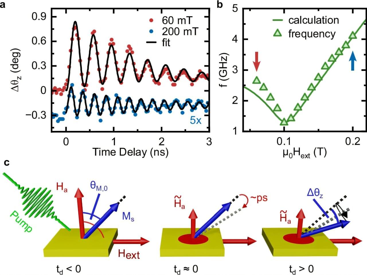
When something draws us in like a magnet, we take a closer look. When magnets draw in physicists, they take a quantum look. Scientists from Osaka Metropolitan University and the University of Tokyo have successfully used light to visualize tiny magnetic regions, known as magnetic domains, in a specialized quantum material. Their study was published in Physical Review Letters.

UC Santa Barbara researchers have achieved the first-ever “movie” of electric charges traveling across the interface of two different semiconductor materials. Using scanning ultrafast electron (SUEM) techniques developed in the Bolin Liao lab, the research team has directly visualized the fleeting phenomenon for the first time.

Researchers have developed a novel graphene-germanium hot-emitter transistor using a new hot carrier generation mechanism, achieving unprecedented performance. This advancement opens new possibilities for low-power, high-performance multifunctional devices.

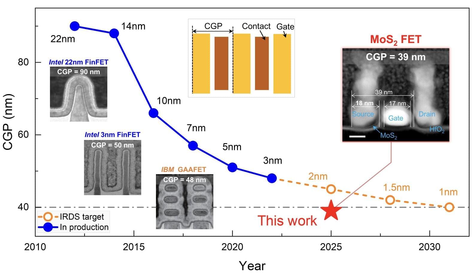
Transistors, the fundamental components of integrated circuits, encounter increasing difficulties as their size continues to shrink. To boost circuit performance, it has become essential to develop transistors that operate on innovative principles. Hot carrier transistors, which harness the extra kinetic energy of charge carriers, offer the potential to enhance transistor speed and functionality. However, their effectiveness has been constrained by conventional methods of generating hot carriers.

A team of researchers led by Prof. Chi Liu, Prof. Dongming Sun, and Prof. Huiming Cheng from the Institute of Metal Research (IMR) of the Chinese Academy of Sciences has proposed a novel hot carrier generation mechanism called “stimulated emission of heated carriers (SEHC).” The team has also developed an innovative hot-emitter transistor (HOET), achieving an ultralow sub-threshold swing of less than 1 mV/dec and a peak-to-valley current ratio exceeding 100. The study provides a prototype of a low-power, multifunctional device for the post-Moore era.

The team of chemists and composite materials researchers discovered a broadly applicable method of bonding plastics and synthetic fibers at the molecular level in a procedure called cross-linking. The cross-linking takes effect when the adhesive is exposed to heat or long-wave UV light making strong connections that are both impact-resistant and corrosion-resistant. Even with a minimal amount of cross-linking, the materials are tightly bonded.

“It turns out the adhesive is particularly effective in high-density polyethylene, which is an important plastic used in bottles, piping, geomembranes, plastic lumber, and many other applications,” says Professor Abbas Milani, director of UBC’s Materials and Manufacturing Research Institute, and the lead researcher at the Okanagan node of the Composite Research Network. “In fact, commercially available glues didn’t work at all on these materials, making our discovery an impressive foundation for a wide range of important uses.”

UVic Organic Chemistry Professor Jeremy Wulff, whose team led the design of the new class of cross-linking materials, collaborated with the UBC Survive and Thrive Applied Research to explore how it performed in real-world applications.

Harder than a diamond, stronger than steel, as flexible as rubber and lighter than aluminum. These are just some of the properties attributed to graphene. Although this material has sparked great interest in the scientific community in recent years, there is still no cheap and sustainable enough method for its high-quality manufacturing on an industrial scale.

After thousands of years as a highly valuable commodity, silk continues to surprise. Now it may help usher in a whole new direction for microelectronics and computing.

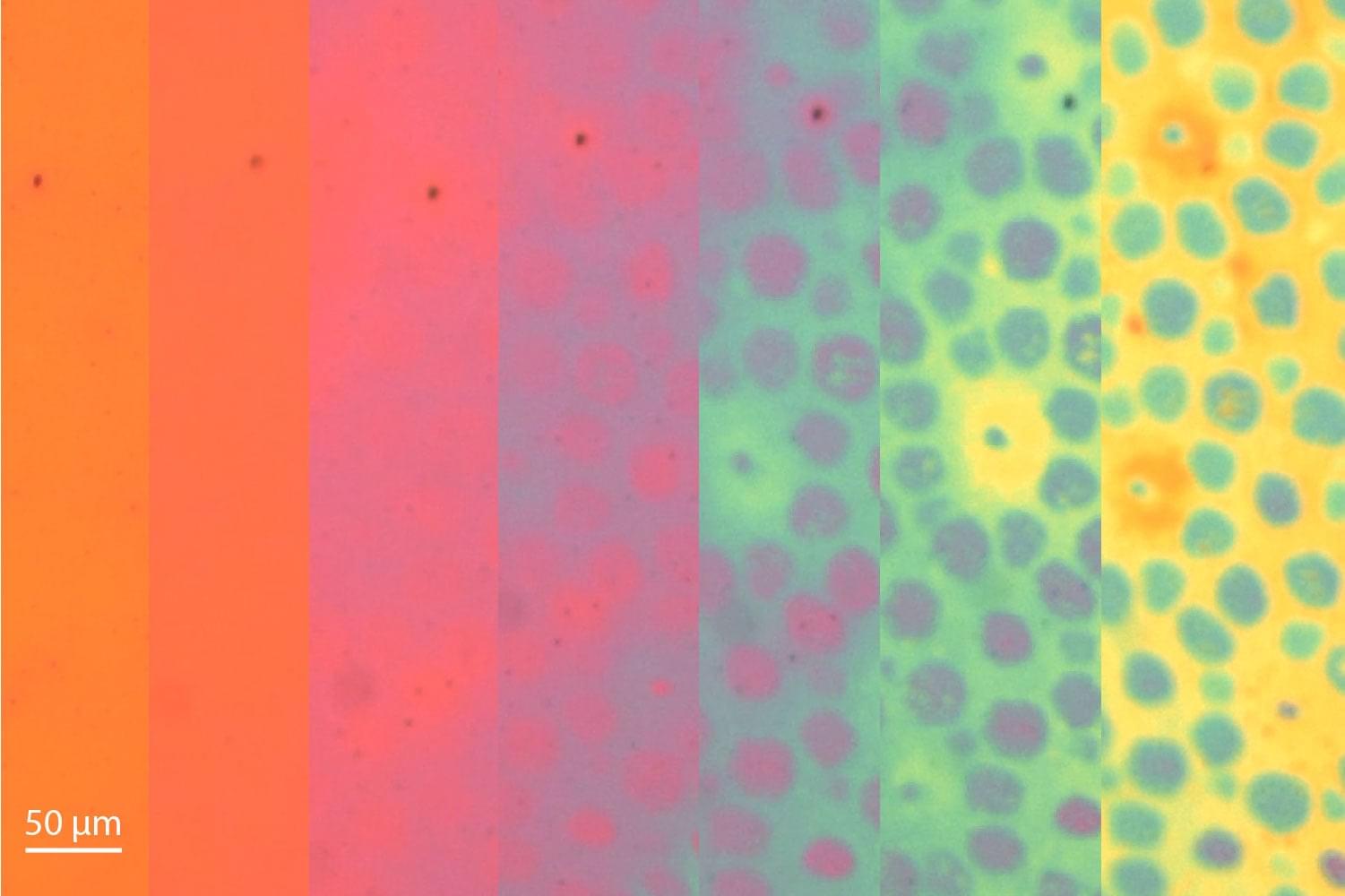
While silk protein has been deployed in designer electronics, its use is currently limited in part because silk fibers are a messy tangle of spaghetti-like strands.

Imagine being able to see electrons — the tiny particles that buzz around atoms — in action, darting and swirling in their frenetic dance. This isn’t science fiction anymore.

Scientists have recently developed a state-of-the-art microscope that allows us to observe these elusive particles moving at unimaginable speeds, revealing the intricate behaviors and interactions that occur at the atomic level.

This innovative technology opens up new frontiers for research in physics and materials science, providing unprecedented insights into the fundamental building blocks of matter.