Toggle light / dark theme

Physicists watch a material’s electrons assemble, and reassemble, into coexisting phases

A tall glass of ice water isn’t just a thirst quencher; it’s also an everyday example of coexisting phases. Water can exist simultaneously in both liquid and solid phases. As it turns out, this phase duality can also exist in more exotic quantum materials, in ways that are far more complicated to tease apart.

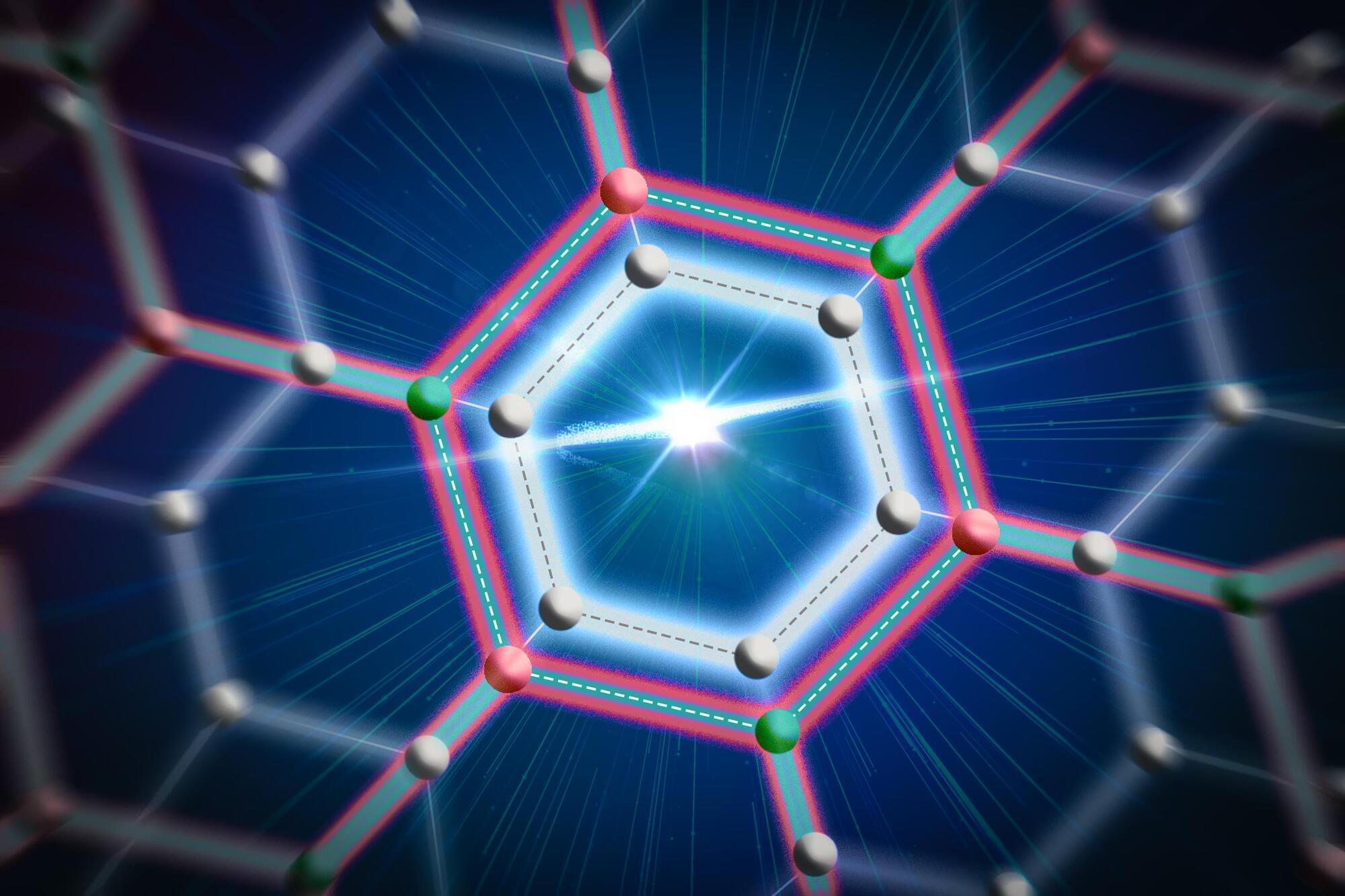
A new study by MIT physicists sheds light on how two different phases of electron behavior can emerge and coexist in the same quantum material.

Their results, reported in the journal Nature Physics, can help explain how some materials host superconductivity, magnetism and other electronic phases. Untangling such phases and understanding how they emerge will help engineers control electronic behavior and design high-performance quantum devices.
Observing key material properties atom by atom for the first time

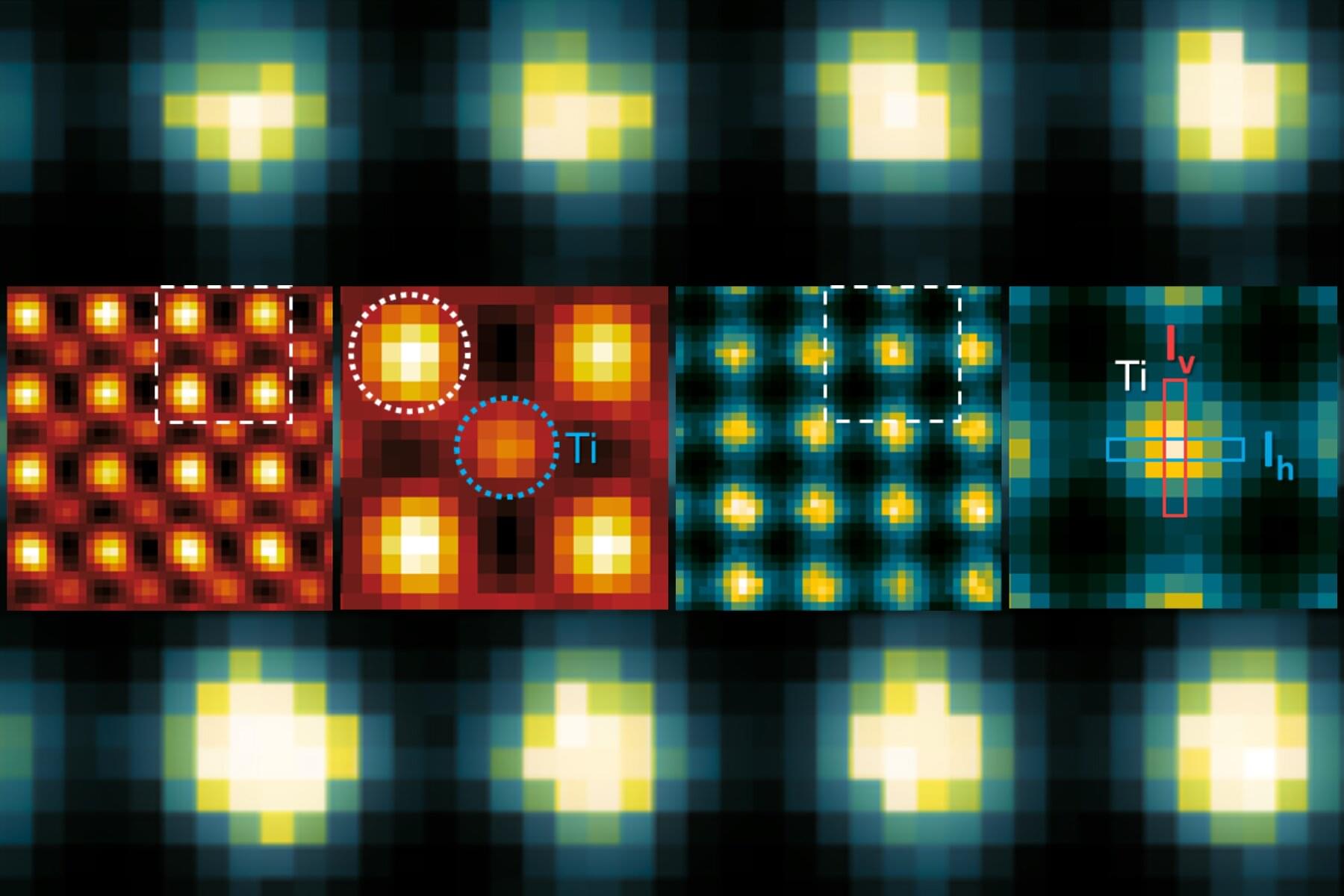
Many material properties depend on how electrons are arranged inside a material. Their distribution determines, for example, whether a material conducts electricity or displays magnetic behavior. Understanding how electrons organize themselves at the atomic scale is therefore one of the major challenges in materials science. Now, a team led by researchers at the Institute of Materials Science of Barcelona (ICMAB-CSIC) has developed a new technique that, for the first time, reveals how electrons are organized inside materials with an unprecedented level of detail.

Until now, available techniques could only provide an overall picture of electronic structure. They could not reveal in detail how electrons vary from one atom to another, either at the surface or deeper within the material. “This type of instrument is like opening a box that until now has been closed,” says Jaume Gàzquez, ICMAB-CSIC researcher and one of the corresponding authors of the paper published in Nature Materials. “We can now observe phenomena that simply could not be seen before.”

The work was carried out in collaboration with the University of the Chinese Academy of Sciences, Uppsala University (Sweden), the University of Washington (United States), and the Pacific Northwest National Laboratory (United States). The project brought together expertise in advanced microscopy, theoretical simulations and materials synthesis.

Never-before-seen woven structure that forms naturally inside a crystal discovered

For the first time, scientists have observed a three-dimensional woven structure forming naturally inside a crystal, revealing a previously unknown way in which matter can organize itself.

Published in Light: Science & Applications, the study reports the observation of a three-dimensional woven fabric of interlaced nano-dipole ensembles that emerges spontaneously in a ferroelectric crystal as it cools through its phase transition. Unlike conventional ferroelectric crystals, in which ferroelectric domains consist of aligned electric dipoles, the dipoles in this material spontaneously weave over and under one another, creating an intricate three-dimensional network that resembles woven fabric—a type of organization never before observed in a solid crystal.

The researchers also found that they could change small parts of the woven network using a tightly focused green laser. The light locally untangles the woven pattern without affecting the rest of the crystal. Heating the crystal and cooling it again restores the woven structure, but with a new pattern.

A new way to watch heat move through electronics

The same overheating problem that happens to our laptops also plagues computer servers and data centers around the world—and heat management is only getting harder as computer chips get more compact and powerful.

Understanding how heat moves through chips at the microscale is essential for continuing to improve their performance. Unfortunately, most methods for measuring heat flow struggle with multilayered devices like the electronics that power our modern world.

Now MIT researchers have demonstrated a new way to study how heat moves through multilayered materials, combining X-rays that penetrate multiple layers with laser pulses to deliver heat. The researchers used the technique to measure how heat moves inside a promising device for transistors and flexible electronics.

Electric field reverses phonon chirality and spin direction in ferroelectric crystal

Chiral phonons are groups of atoms that move in a circular direction when excited by an energy source, such as heat. As the phonons move through a material, they propagate that circular motion, or angular momentum, through the material. The angular momentum serves as the source of spin, and the chirality dictates the direction of the spin, enabling spin control in spintronics.

Chirality, in simple terms, means that a molecule or material cannot be superimposed on its mirror image—think of your left and right hands, for example. A left-handed glove does not fit on your right hand, and vice versa.

In a new study, researchers used an electric field to switch the chirality of phonons within a ferroelectric crystal. The work could lead to the creation of faster and more energy-efficient spintronic devices.

Scientists just 3D printed one of the hardest metals on Earth

The results provide a foundation for further development, but several challenges remain. The researchers want to reduce cracking, improve durability, and determine how to manufacture more complicated shapes.

“The approach of forming metal materials by softening them rather than fully melting them is novel, and it has the potential to be applied not only to cemented carbides, which were the focus of this study, but also to other materials,” said Marumoto.

New approach to cleaning the inner walls of a fusion system removes another obstacle to near-endless energy

Fusion systems need inner walls that can withstand extreme heat. One promising solution uses liquid lithium to protect the walls, held like water in a sponge made of the exceptionally strong metal tungsten. An advanced manufacturing process can be used to make tungsten into sponge-like wall tiles with lots of pores for flowing liquid lithium. But this process also leaves the tungsten contaminated with other materials, such as carbon, oxygen or nitrogen.

When exposed to liquid lithium, the carbon and oxygen react to form solids that can plug the holes in the tungsten, preventing the lithium from flowing properly. Even if the tungsten were cleaned at the end of the manufacturing process, it would become recontaminated when the tiles are exposed to air during installation.

Now researchers from the U.S. Department of Energy’s Princeton Plasma Physics Laboratory (PPPL), Princeton University and Pennsylvania State University have found a clever way to clean those tiles after they are installed and sealed inside the fusion system—in vacuum chambers from which the air has been removed. The advance, which uses heat combined with particles from a neon plasma to knock contaminants out of tiles, could help future fusion systems run better with liquid lithium.

Two materials, one photonic chip: Unlocking a new way to generate light frequencies

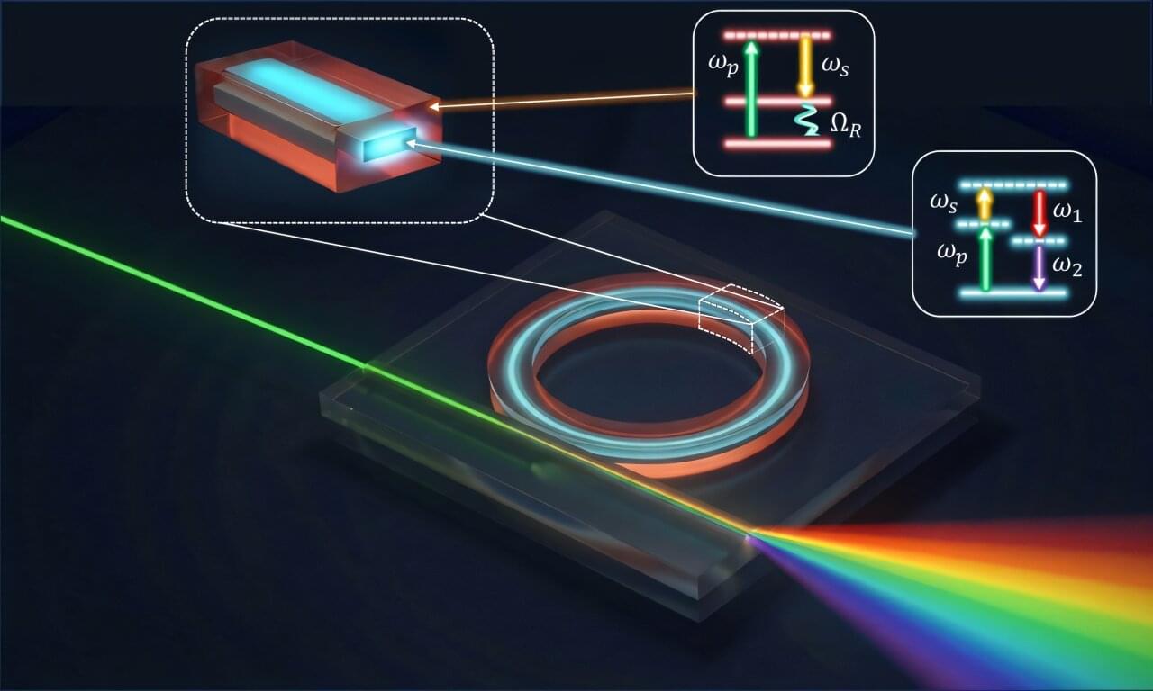
Modern photonic chips can pack sophisticated optical functions onto devices smaller than a fingernail. They are increasingly used to generate, manipulate and measure light for applications ranging from communications to sensing. But most of these chips rely on a single material to do the heavy lifting, limiting the range of optical effects they can produce.

Researchers have now demonstrated a different approach: letting two materials share the work. As reported in Advanced Photonics, scientists combined two nonlinear optical effects that normally occur separately. Their device uses a silicon nitride core to generate optical frequency combs while a surrounding silica layer produces Raman scattering.

By harnessing the strengths of both materials at once, the team created a new type of integrated photonic device capable of generating broad ranges of light frequencies on a chip.