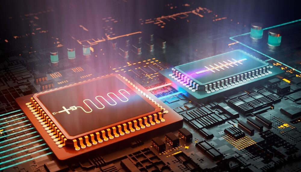
Chasing ever-higher qubit counts in near-term quantum computers constantly demands new feats of engineering.
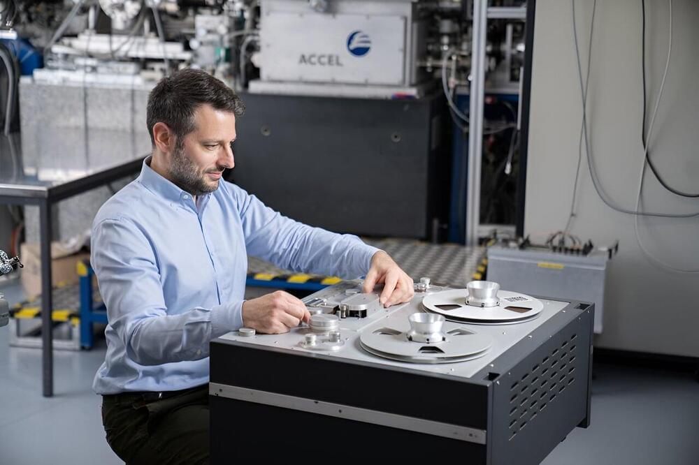
Researchers are developing a technique that uses the special synchrotron X-ray light from the Swiss Light Source SLS to non-destructively digitize recordings from high-value historic audio tapes—including treasures from the Montreux Jazz Festival archive, such as a rare recording of the King of the Blues, B.B. King.
Magnetic tapes have almost completely disappeared from our lives and now only enjoy a nostalgic niche existence. However, significant quantities of these analog magnetic media are still stored in the archives of sound studios, radio and TV stations, museums, and private collections worldwide. Digitizing these tapes is an ongoing challenge as well as a race against time, as the tapes degrade and eventually become unplayable.
Sebastian Gliga, physicist at PSI and expert in nanomagnetism, and his team are developing a method to non-destructively digitize degraded audio tapes in the highest quality using X-ray light. To achieve this goal, they have been collaborating with the Swiss National Sound Archives, which has produced custom-made reference recordings and provided audio engineering know-how. Now, a partnership with the Montreux Jazz Digital Project will help to further develop and test the method.

Professor Jiyun Kim and his team at the Department of Material Science and Engineering at Ulsan National Institute of Science and Technology (UNIST) have developed a pioneering technology capable of identifying human emotions in real time. This cutting-edge innovation is set to revolutionize various industries, including next-generation wearable systems that provide services based on emotions.
Understanding and accurately extracting emotional information has long been a challenge due to the abstract and ambiguous nature of human affects such as emotions, moods, and feelings. To address this, the research team has developed a multi-modal human emotion recognition system that combines verbal and non-verbal expression data to efficiently utilize comprehensive emotional information.
Engineering the tunability of protein assembly in response to pH changes within a narrow range is challenging. Here the authors report the de novo computational design of pH-responsive protein filaments that exhibit rapid, precise, tunable and reversible assembly and disassembly triggered by small pH changes.
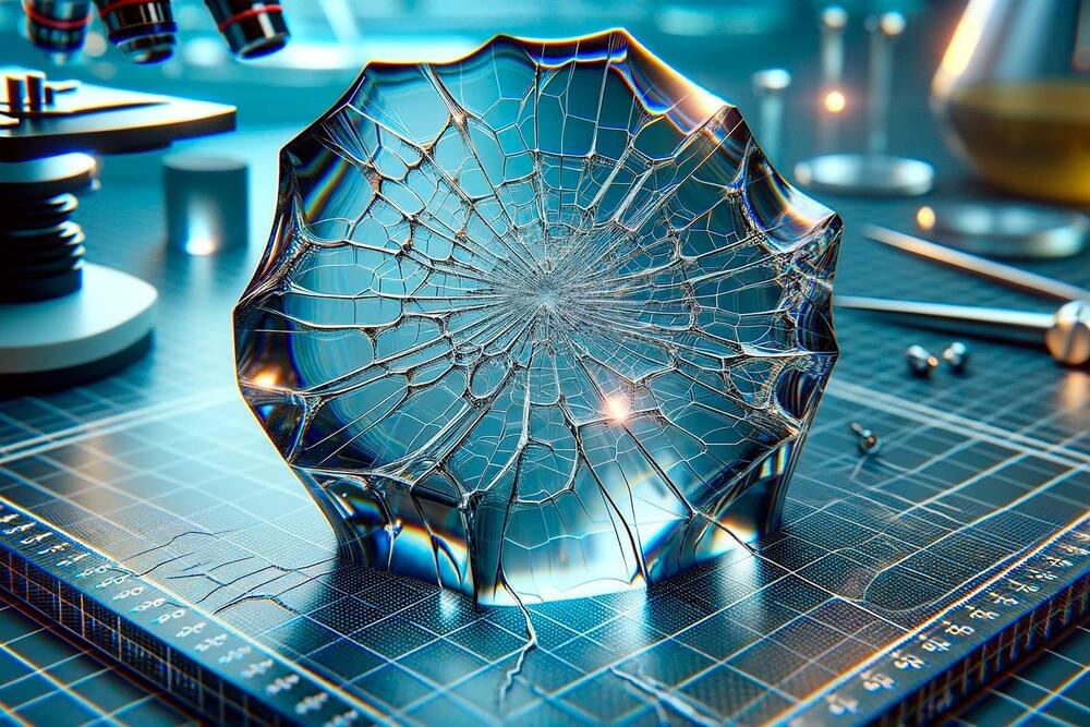
The last time you dropped a favorite mug or sat on your glasses, you may have been too preoccupied to take much notice of the intricate pattern of cracks that appeared in the broken object. But capturing the formation of such patterns is the specialty of John Kolinski and his team at the Laboratory of Engineering Mechanics of Soft Interfaces (EMSI) in EPFL’s School of Engineering. They aim to understand how cracks propagate in brittle solids, which is essential for developing and testing safe and cost-effective composite materials for use in construction, sports, and aerospace engineering.
Southwest Research Institute has invested in research to enhance the capabilities of spacecraft instruments. Consequently, they have developed more effective conversion surfaces for the detection and analysis of low-energy particles in outer space.
Led by Dr. Jianliang Lin of Mechanical Engineering and Dr. Justyna Sokół of the Space Science Division, the project could potentially change our understanding of space physics and exploration.
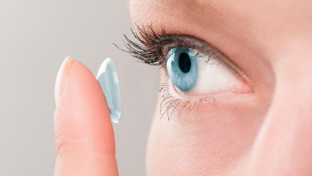
Conventionally, corneal abrasion patients wear a clear, oxygen-permeable bandage contact lens for seven to 10 days but this treatment does not ensure the drug remains in the eye for sustained treatment, according to a statement by the University of Waterloo.
This new lens material was developed with the ambition to address the limitations of current methods for treating corneal abrasions. The contact lens material is derived from gelatin methacrylate, a collagen by-product. Collagen is a protein naturally found in the eye and is involved in the wound-healing process but it’s too soft and weak to perform as an appropriate contact lens material.
Dr. Evelyn Yim, an associate professor of chemical engineering at the University of Waterloo, found a way to transform gelatin methacrylate into a biomaterial ten times stronger than collagen, the statement revealed.
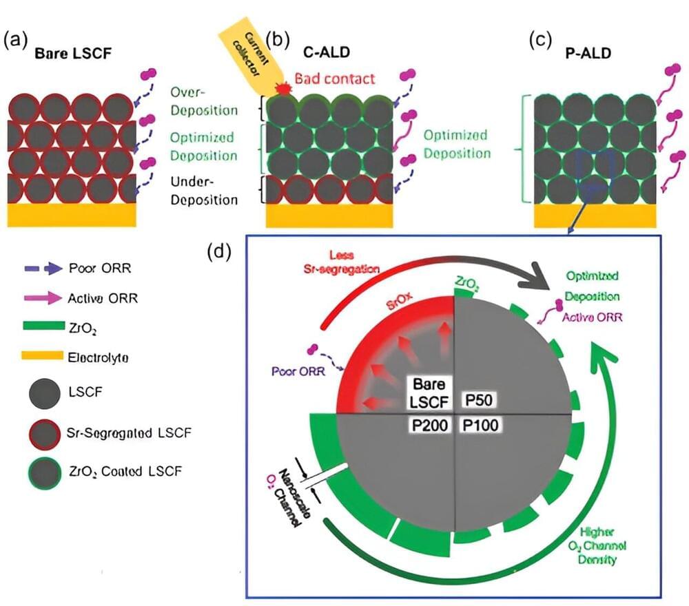
To enhance this efficiency, there is a requirement to fabricate electrodes with a porous structure. Unfortunately, existing technologies face challenges in achieving a uniform coating of ceramic materials within electrodes possessing intricate porous structures.
A collaborative research team, comprising Professor Jihwan An and Ph.D. candidate Sung Eun Jo from the Department of Mechanical Engineering at Pohang University of Science and Technology (POSTECH), and others, has successfully produced porous electrodes for SOFCs using latest semiconductor processes. This research has been featured as a back cover article in Small Methods.
The process of atomic layer deposition (ALD) involves depositing gaseous materials onto a substrate surface in thin, uniform atomic layers. In a recent study, Professor Jihwan An’s team, known for their prior work in enhancing the efficiency of SOFCs using ALD, developed and applied a powder ALD process and equipment. This enabled them to precisely coat nano-thin films on fine powders.