Toggle light / dark theme

Nanoelectronics.


This new feature in Nano TV will present the best of science and technology in a short format, which is easy to understand and also appreciate the beauty of scientific knowledge. Catering to all, these shorts will be informative and educative. Explore science, explore Nanotechnology through our latest series called Nano Shorts.

Nanotechnology is the buzz of the world today. Here are some lesser-known facts about this emerging technology:

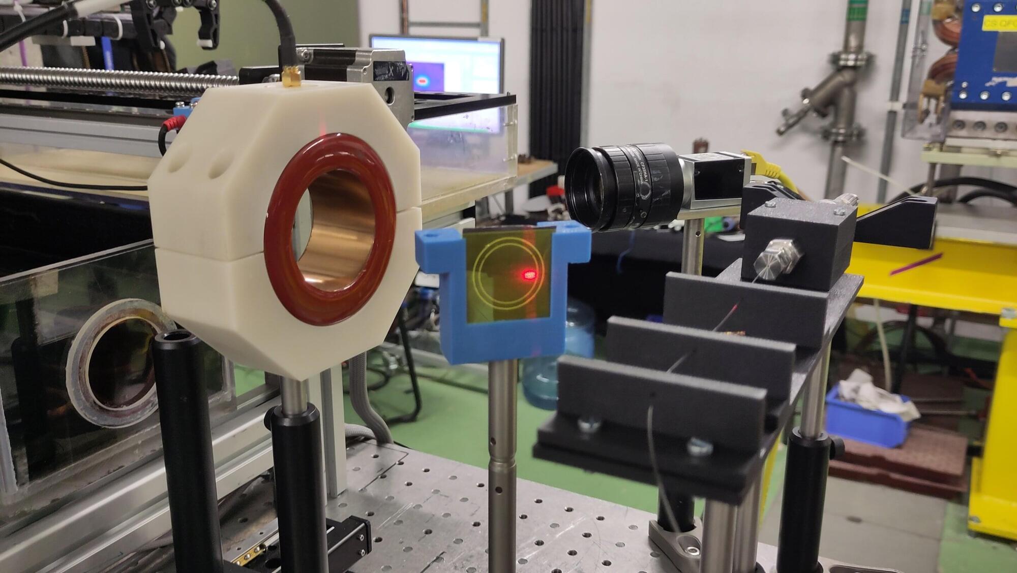
A new NASA-funded study has revealed for the first time that the airflow in supersonic combusting jet engines can be controlled by an optical sensor.

The finding can lead to more efficient stabilization of hypersonic jet aircraft, according to the study carried out by the researchers at the University of Virginia, School of Engineering and Applied Science.

The research allows operators to control airflow at the speed of light when a ‘shock train’ occurs. A shock train is a condition that precedes engine failure within a scramjet engine.

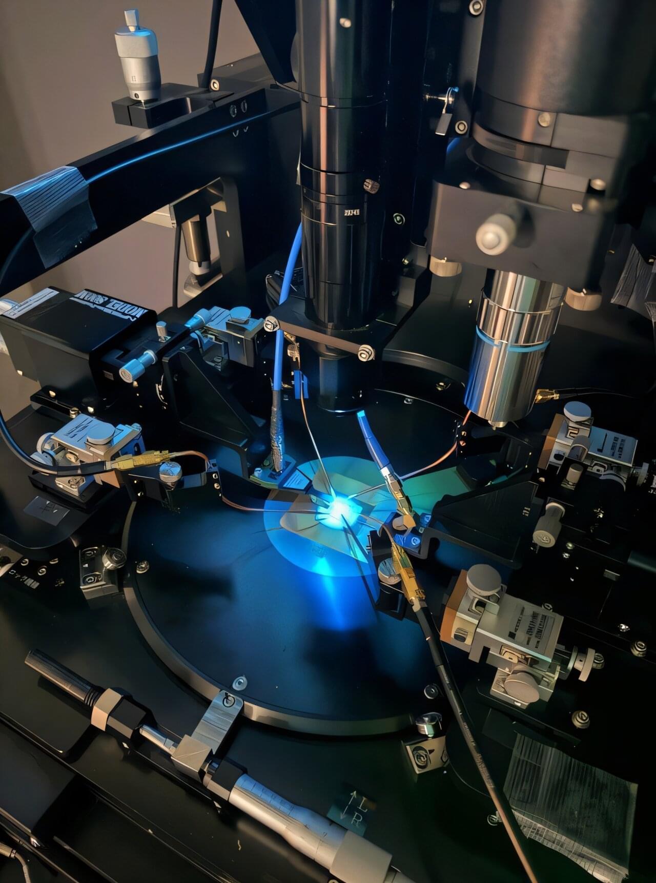
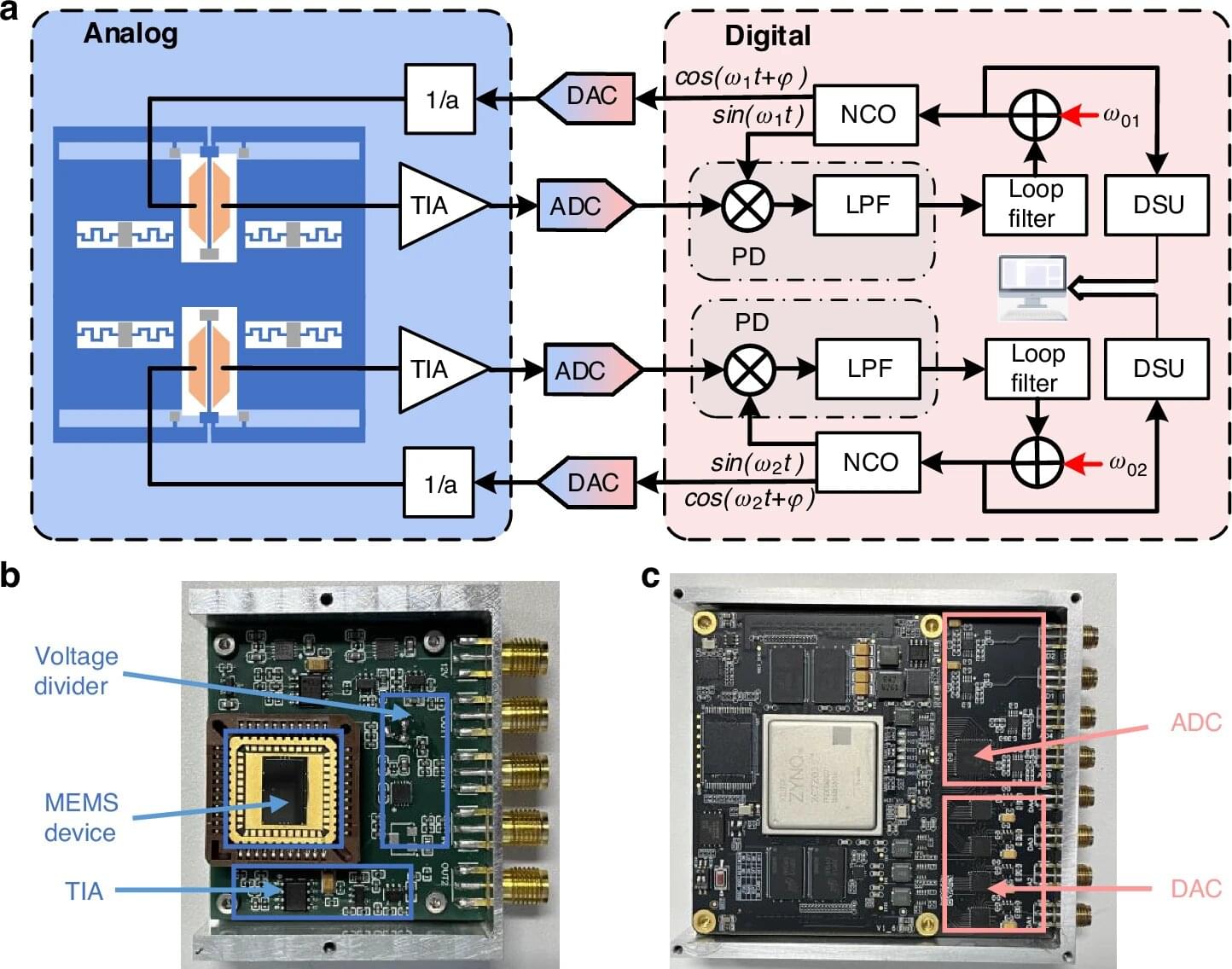
In recent years, physicists and engineers have developed increasingly sophisticated instruments to study particles and the interactions between them with high precision. These instruments, which include particle detectors, sensors and accelerometers, could help researchers to study physical processes in greater detail, potentially contributing to interesting new discoveries.

A team of researchers from ANSTO and University of Technology Sydney have set a record by conducting thin film experiments at 1,100 degrees Celsius, using the Spatz reflectometer equipped with a vacuum furnace.

The unique combination of neutron reflectometry with high temperature apparatus enables atomic-scale insights into thin film growth and diffusion processes. This is of relevance to a wide range of thin film technology and devices which undergo a range of processing and heat treatment conditions to optimize performance.

The UTS group, led by Francesca Iacopi and Aiswarya Pradeepkumar, has been studying the growth of thin carbon sheets (graphene) on SiC/Si substrates which occurs at high temperatures. This award-winning process allows for highly conductive electronics that can be integrated with standard silicon fabrication processes.

Silicon, the cornerstone of modern electronics, photovoltaics, and photonics, has traditionally been limited to surface-level nanofabrication due to the challenges posed by existing lithographic techniques. Available methods either fail to penetrate the wafer surface without causing alterations or are limited by the micron-scale resolution of laser lithography within Si.