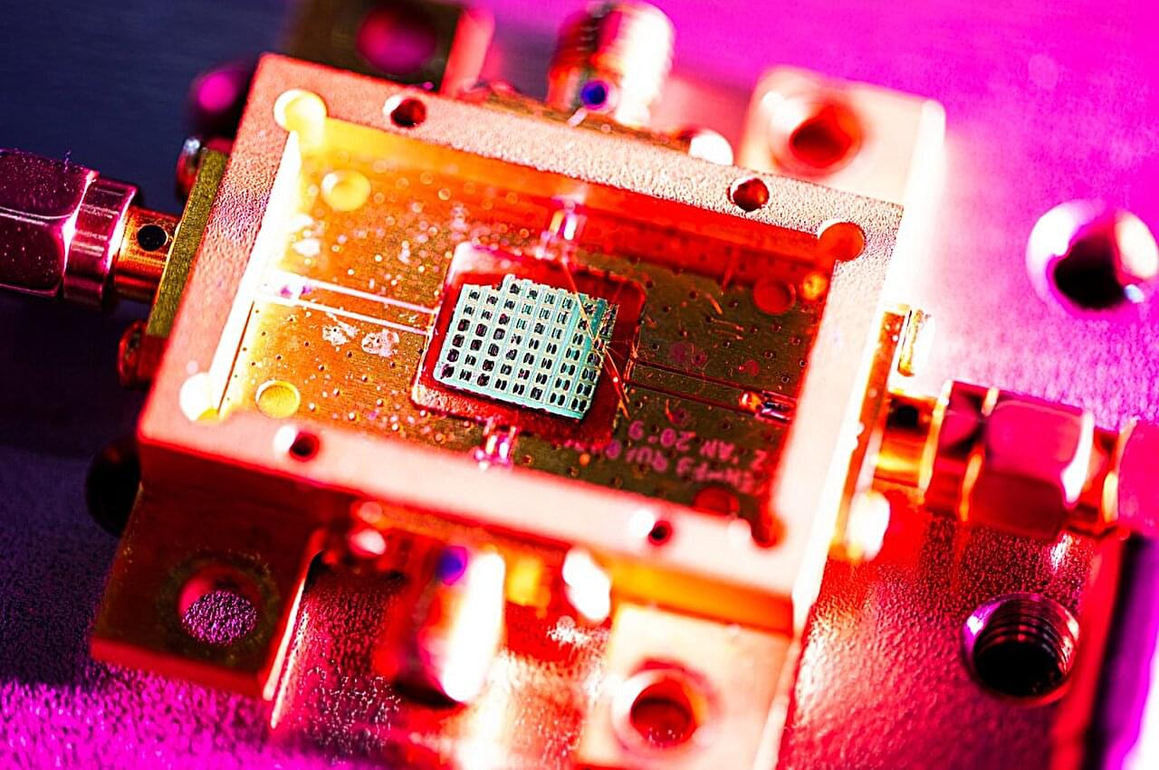
Toggle light / dark theme

Today’s computers reach their physical limits when it comes to speed. Semiconductor components usually operate at a maximum usable frequency of a few gigahertz – which corresponds to several billion computing operations per second. As a result, modern systems rely on several chips to divide up the computing tasks because the speed of the individual chips cannot be increased any further. However, if light (photons) were used instead of electricity (electrons) in computer chips, they could be up to 1,000 times faster.

Plasmonic resonators, also known as “antennas for light”, are a promising way of achieving this leap in speed. These are nanometre-sized metal structures in which light and electrons interact. Depending on their geometry, they can interact with different light frequencies.

“The challenge is that plasmonic resonators cannot yet be effectively modulated, as is the case with transistors in conventional electronics. This hinders the development of fast light-based switches,” says Dr. Thorsten Feichtner, physicist at Julius-Maximilians-Universität (JMU) Würzburg in Bavaria, Germany.

A research team has identified key visual perceptual factors that enhance the viewing experience of 3D displays.

The research revealed that the presence of parallax significantly impacts the perceived realism and immersion of 3D images viewed through .

The results of this study were published in ACM Transactions on Graphics on July 19, and were presented at the international conference on , SIGGRAPH 2024, held in Denver from July 28 to August 1.

Researchers at Leibniz University Hannover have developed a technology for transmitting entangled photons through optical fibers, which could enable the integration of quantum and conventional internet, promising enhanced security and efficient use of existing infrastructure.

A team of four researchers from the Institute of Photonics at Leibniz University Hannover has developed an innovative transmitter-receiver system for transmitting entangled photons via optical fiber.

This breakthrough could enable the next generation of telecommunications technology, the quantum Internet, to be routed via optical fibers. The quantum Internet promises eavesdropping-proof encryption methods that even future quantum computers cannot decrypt, ensuring the security of critical infrastructure.

Two-dimensional (2D) semiconducting materials have distinct optoelectronic properties that could be advantageous for the development of ultra-thin and tunable electronic components. Despite their potential advantages over bulk semiconductors, optimally interfacing these materials with gate dielectrics has so far proved challenging, often resulting in interfacial traps that rapidly degrade the performance of transistors.

Researchers at King Abdullah University of Science and Technology (KAUST), Soochow University and other institutes worldwide recently introduced an approach that could enable the fabrication of better performing transistors based on 2D semiconductors. Their proposed design, outlined in a paper in Nature Electronics, entails the use of hexagonal boron nitride (h-BN) dielectrics and metal gate electrodes with a high cohesive energy.

“Initially, we found that when we use platinum (Pt) as an anode, the h-BN stack is less likely to trigger breakdown,” Yaqing Shen, first author of the paper, told Tech Xplore. “Based on this finding, we designed our experiments and found that Pt/h-BN gate stacks show 500-times lower leakage current than Au/h-BN gate stacks and exhibit a high dielectric strength of at least 25 MV/cm. This gave us the idea of using CVD h-BN as a gate dielectric in 2D transistors.”

Research teams from Wuhan University and the China University of Geosciences (Wuhan) have revealed new insights into the formation mechanism of nitrogen-vacancies (NV) centers in type-Ib diamonds, a phenomenon critical to quantum sensing and computing advancements. Using a novel irradiation and annealing method, the teams demonstrated how controlled temperature and orientation can significantly increase the density and depth of NV centers, paving the way for new applications in biological imaging and quantum technologies.

Learning and a spectrum of other behavioral competencies allow organisms to rapidly adapt to dynamically changing environmental variations. The emerging field of diverse intelligence seeks to understand what systems, besides ones with complex brains, exhibit these capacities. Here, we tested predictions of a general computational framework based on the free energy principle in neuroscience but applied to aneural biological process as established previously, by demonstrating and manipulating pattern recognition in a simple aneural organism, the green algae Volvox. Our studies of the adaptive photoresponse in Volvox reveal that aneural organisms can distinguish between patterned and randomized inputs and indicate how this is achieved mechanistically.

A newly developed transistor device has shown exceptional levels of resilience in tests, performing so well, in fact, that it promises to transform the electronics and gadgets we make use of each day.

These tiny toggles are essential in just about every modern day electronic device, involved in storing data and processing information in a binary ‘on’ or ‘off’ state, switching back and forth multiple times a second.

Thanks to its remarkable combination of speed, size, and resilience to wear, this latest design potentially represents a huge upgrade for consumer devices like phones and laptops, as well as the data centers that store all of our information in the cloud.